Connection Test Output


In previous steps of the tutorial, you have categorised all the devices that are connected, both directly and indirectly, to JTAG enabled devices in the circuit. You can not only run tests on those devices, but you have also maximised the test coverage achieved by the Connection Test.
In this step of the tutorial, you will see the types of fault that can be detected by the Connection Test, and the way they are reported.
- Click
 Run Tests under the Run and Deploy.
 - Click
 Presets at the bottom of the Test List on the right side of the screen, and select
  None.
None. - Double-click the Connection Test group name in the Test List to re-enable that test.
Open circuit faults
An open circuit error can be created on the XJDemo board using FCJ1.
- Remove the jumper marked JTAG Open on FCJ1, which is highlighted in the picture below.
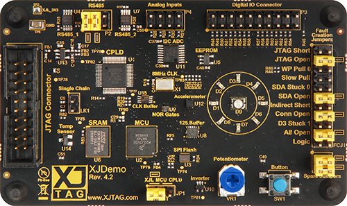
This breaks a connection between the two JTAG devices.
- Click
 Run to run the Connection Test and you will see the following output:
Selecting profile 'All chains'...
Performing standard Connection Test...
Generating Connection Test data...
Performing Logic Tests (phase 1)...
Performing Logic Tests (phase 2)...
Analysing Connection Test results...
Analysing Logic Tests (phase 1)...
Analysing Logic Tests (phase 2)...
Error on net COMMS_INT-COMMS_INTa: Open circuit error between the JTAG pins.
Net Detail
Net COMMS_INT-COMMS_INTa contains:
-
Linked net COMMS_INT
- FCJ1.3 (PASSIVE)
- TP76.1 (UNFITTED)
- U2.B4(PTC18) (JTAG)
-
Linked net COMMS_INTa
- FCJ1.4 (PASSIVE)
- U1.64(IO64) (JTAG)
Error Detail
| U2.B4 | U1.64 | |||
|---|---|---|---|---|
| W | R | W | R | |
| 0 | - | 0 | 0 | 0 |
| 1 | - | 0 | 1 | 1 |
| 2 | - | 0 | 0 | 0 |
| 3 | - | 0 | 1 | 1 |
| 4 | - | 0 | - | 1 |
| 5 | - | 0 | - | 1 |
| 6 | - | 0 | - | 1 |
| 7 | - | 0 | - | 1 |
| 8 | - | 0 | 0 | 0 |
| 9 | - | 0 | 1 | 1 |
| 10 | - | 0 | 0 | 0 |
| 11 | - | 0 | 1 | 1 |
| 12 | - | 0 | - | 1 |
| 13 | - | 0 | - | 1 |
| 14 | - | 0 | - | 1 |
| 15 | - | 0 | - | 1 |
| 16 | - | 0 | - | 1 |
| 17 | - | 0 | - | 1 |
| 18 | - | 0 | - | 1 |
| 19 | - | 0 | - | 1 |
| 20 | - | 0 | - | 1 |
| 21 | - | 0 | - | 1 |
| 22 | - | 0 | - | 1 |
| 23 | - | 0 | - | 1 |
| 24 | - | 0 | - | 1 |
| 25 | - | 0 | - | 1 |
| 26 | - | 0 | - | 1 |
| 27 | - | 0 | - | 1 |
| 28 | - | 0 | 0 | 0 |
| 29 | - | 0 | 1 | 1 |
| 30 | - | 0 | 0 | 0 |
| 31 | - | 0 | 1 | 1 |
| 32 | - | 1 | - | 1 |
| 33 | - | 1 | - | 1 |
| 34 | - | 1 | - | 1 |
| 35 | - | 1 | - | 1 |
| 36 | - | 1 | 0 | 0 |
| 37 | - | 1 | 1 | 1 |
| 38 | - | 1 | 0 | 0 |
| 39 | - | 1 | 1 | 1 |
| 40 | 0 | 0 | - | 1 |
| 41 | 1 | 1 | - | 1 |
| 42 | 0 | 0 | - | 1 |
| 43 | 1 | 1 | - | 1 |
| 44 | 0 | 0 | - | 1 |
| 45 | 1 | 1 | - | 1 |
| 46 | 0 | 0 | - | 1 |
| 47 | 1 | 1 | - | 1 |
1 error
CONNTEST failed - ran in default profile (All chains)
>>>> FAILED <<<<
| NAME | RESULT | SUMMARY | TIME |
|---|---|---|---|
| Connection Test - using default profile |
Failed | 0.528 | |
| TOTAL TIME | 0.528 |
To find out more about the data used to diagnose this fault, expand the Error Detail:
- Click the next to Error Detail in the Connection Test output.
Due to the nature of open-circuit faults there can be an element of randomness in the data read on a net with such a fault, and therefore the error details you see may not look exactly as shown above.
In the case of an open circuit error, each column of information represents a JTAG enabled pin on a net; within each of these columns the write and read values for each test step is displayed. Where there is a '-' (hyphen) in the write column it means that no data was written to that pin during that test step, i.e. it was high-impedance.
You can see in the Error Detail that in the first four steps of the Connection Test the net was being driven by pin 64 on U1 and while that pin read back the expected values, the other pin on the net, U2.B4, read back a 0. The blue highlighting of these test steps means that this data was not what was expected. In this case the data has been analysed and found to be consistent with open circuit behaviour.
In the next four steps nothing was written to either of the JTAG enabled pins on this net, though this does not mean that nothing was happening. When a net is high-impedance it is being monitored to see if it reads back the values driven to other nets in the circuit, in order to detect short circuit faults.
- Re-fit the jumper to FCJ1 to resolve the open circuit fault.
Short circuit faults
You can also use FCJ1 to create a short circuit fault between JTAG enabled nets on the XJDemo board:
- Use one of the Spare Jumpers (on the XJDemo board they are located below the Fault Creation Jumpers) to create the fault marked as JTAG Short on FCJ1 – see picture.
- Run the Connection Test again.
- Click the next to Net Detail to show the pins on the nets that are shorted together.
Error: Short found between nets: IO19-NetP3_19, LED9_R.
Net Detail
Net IO19-NetP3_19 contains:
- Linked net IO19
- FCJ1.2
- R64.1
- U1.34(IO34)
- Linked net NetP3_19
- P3.19
- R64.2
Net LED9_R contains:
- D9.1
- FCJ1.1
- TP45.1
- U1.33(IO33)
Error Detail
| IO19-NetP3_19 | LED9_R | |||
|---|---|---|---|---|
| W | R | W | R | |
| 0 | - | 1 | - | 1 |
| 1 | - | 1 | - | 1 |
| 2 | - | 1 | - | 1 |
| 3 | - | 1 | - | 1 |
| 4 | 0 | 0 | - | 0 |
| 5 | 1 | 1 | - | 1 |
| 6 | 0 | 0 | - | 0 |
| 7 | 1 | 1 | - | 1 |
| 8 | 0 | 0 | 0 | 0 |
| 9 | 1 | 1 | 1 | 1 |
| 10 | 0 | 0 | 0 | 0 |
| 11 | 1 | 1 | 1 | 1 |
| 12 | - | 0 | 0 | 0 |
| 13 | - | 1 | 1 | 1 |
| 14 | - | 0 | 0 | 0 |
| 15 | - | 1 | 1 | 1 |
| 16 | - | 1 | - | 1 |
| 17 | - | 1 | - | 1 |
| 18 | - | 1 | - | 1 |
| 19 | - | 1 | - | 1 |
| 20 | - | 0 | 0 | 0 |
| 21 | - | 1 | 1 | 1 |
| 22 | - | 0 | 0 | 0 |
| 23 | - | 1 | 1 | 1 |
| 24 | - | 1 | - | 1 |
| 25 | - | 1 | - | 1 |
| 26 | - | 1 | - | 1 |
| 27 | - | 1 | - | 1 |
| 28 | 0 | 0 | 0 | 0 |
| 29 | 1 | 1 | 1 | 1 |
| 30 | 0 | 0 | 0 | 0 |
| 31 | 1 | 1 | 1 | 1 |
| 32 | - | 0 | 0 | 0 |
| 33 | - | 1 | 1 | 1 |
| 34 | - | 0 | 0 | 0 |
| 35 | - | 1 | 1 | 1 |
| 36 | 0 | 0 | - | 0 |
| 37 | 1 | 1 | - | 1 |
| 38 | 0 | 0 | - | 0 |
| 39 | 1 | 1 | - | 1 |
| 40 | - | 1 | - | 1 |
| 41 | - | 1 | - | 1 |
| 42 | - | 1 | - | 1 |
| 43 | - | 1 | - | 1 |
| 44 | - | 1 | - | 1 |
| 45 | - | 1 | - | 1 |
| 46 | - | 1 | - | 1 |
| 47 | - | 1 | - | 1 |
The Net Detail shows every pin on each of the two nets involved, and nets linked to those. In this case there are two pairs of pins (one on each net) which might be candidates to be shorted to each other:
- U1 – pins 33 and 34
- FCJ1 – pins 1 and 2
It is not always easy to see these potential error locations if the nets have a large number of pins.
However, because this project uses ODB++ data as the netlist for the board, each Connection Test error has a link to XJTAG's Layout Viewer, allowing you to visualise the information.
- Click Short found between nets to view these two nets in the
 Layout Viewer.
As shown below, the Layout Viewer is opened with both nets IO19-NetP3_19 and LED9_R highlighted.
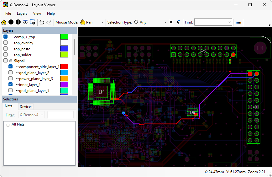
In the image above, the tracks on the top layer of the PCB are shown in red, the tracks on the bottom layer are shown in blue, and the tracks on an internal layer are shown in purple. The Layout Viewer will automatically show all the layers that contain tracks for the selected nets. To change the default layer colours, see the Layout Viewer Help for Layers.
Where you have physical access you can check each of these parts of the board to find the short. In this case the fault is very likely to be at U1 or FCJ1 as the two nets do not come physically close to each other on the same layer at any other points (unless there was a fault in the bare PCB).
Schematic Viewer
When there are schematics linked to boards in a project, it is possible to open the schematic via the links for single devices, pins and nets.
- Return to the Run Tests screen in XJDeveloper.
- Click the next to Net Detail to expand that section of the error output that is still shown on the screen.
- Right-click U1.34 in the test results window and click
 Show in Schematic Viewer.
The Schematic Viewer is launched and the first match for the link is highlighted on the page. From here, you can quickly cycle through all matches for the link using the  Next and
  Previous buttons, and zoom in or out to get a better understanding of the part of the circuit where the fault has been detected.
- Remove the jumper from FCJ1 to resolve the short circuit fault.
Logic Errors
Logic errors are diagnosed by exercising the Logic devices that have been categorised in the circuit. On the XJDemo board there are three devices that will be tested in this way during the Connection Test:
- U8 – a 74LVC125A tri-stateable buffer.
- U9 – a 74LVC2G02GS dual NOR gate.
- U10 – a 74LVC1G04SE inverter.
There is another Logic device on the XJDemo board (U15, a clock fan-out buffer) but that cannot be tested in the Connection Test. It will be tested using an XJEase Test Device File.
A fault involving a Logic device can be introduced to the XJDemo board using FCJ1.
- Use one of the Spare Jumpers to create the fault marked as Logic on the Fault Creation Jumpers FCJ1 – see picture.
- Run the Connection Test again.
- Click the next to Error Detail to show the values driven into and read from the Logic devices.
Error: Unexpected value on logic net DECODE.
Net Detail
Net DECODE contains:
- TP21.1
- U1.24(IO24)
- U9.7
Error Detail
Displaying data from Logic tests (phase 1)
| JTAG Data | Related Logic Block Data | ||||||||||
|---|---|---|---|---|---|---|---|---|---|---|---|
| Pin | U1.24 | U10.2 | U9.2 | U9.7 | NetR40_1-nA17 | ||||||
| Net | DECODE | A17 | A16 | DECODE | NetR40_1-nA17 | ||||||
| W | R | W | R | W | R | W | R | W | R | ||
| 0 | - | 0 | 1 | 1 | 1 | 1 | (0) | 0 | (0) | - | |
| 1 | - | 1 | 1 | 1 | 0 | 0 | (1) | 1 | (0) | - | |
| 2 | - | 1 | 0 | 0 | 0 | 0 | (0) | 1 | (1) | - | |
| 3 | - | 0 | 0 | 0 | 1 | 1 | (0) | 0 | (1) | - | |
| 4 | - | 1 | 0 | 0 | 0 | 0 | (0) | 1 | (1) | - | |
| 5 | - | 1 | 0 | 0 | 0 | 0 | (0) | 1 | (1) | - | |
| 6 | - | 1 | 0 | 0 | 0 | 0 | (0) | 1 | (1) | - | |
| 7 | - | 1 | 0 | 0 | 0 | 0 | (0) | 1 | (1) | - | |
| 8 | - | 1 | 0 | 0 | 0 | 0 | (0) | 1 | (1) | - | |
| 9 | - | 1 | 0 | 0 | 0 | 0 | (0) | 1 | (1) | - | |
| 10 | - | 0 | 1 | 1 | 1 | 1 | (0) | 0 | (0) | - | |
| 11 | - | 1 | 1 | 1 | 0 | 0 | (1) | 1 | (0) | - | |
| 12 | - | 1 | 0 | 0 | 0 | 0 | (0) | 1 | (1) | - | |
| 13 | - | 0 | 0 | 0 | 1 | 1 | (0) | 0 | (1) | - | |
Faults related to Logic devices are more complex than simple short-circuit or open-circuit faults. In this case the NOR gate U9 has two inputs: one is directly connected to the JTAG enabled MCU, U2, while the other is connected to the inverter U10 which is, in turn, connected to U2. The output from the NOR gate can then be sampled at JTAG enabled CPLD U1.
In the Error Detail you can see that there are two sections. The first part of the table (to the left) contains the JTAG pins that are on the net where the error was identified. In this case there is only one JTAG pin, on net DECODE. The second part of the table contains the pins and nets on the logic device(s) that were used as part of the test, including the pin where the error was detected.
The rows highlighted blue in Error Detail contain information indicating a problem in this logic block. By reviewing the highlighted rows and identifying the columns where written (W) and read (R) values differ, you can pinpoint the source of the fault.
Examining the first highlighted row for the error detected on net DECODE, it is only the U9.7 column where the W and R values do not match. The brackets around the W value in this column indicate that, at this point of testing, the net is expected to be driven to that value by a Logic device. The write value of the DECODE net is a logic Low but it is being read as a logic High. The U10.2 and U9.2 columns have no brackets as they are being directly driven and read from a JTAG device. The final column for net NetR40_1-nA17 has a bracketed W value as this net is driven by the inverter. It has a '-' (hyphen) for its R value as the Connection Test has no way of reading the net.
The fact that the DECODE net does read both logic High and logic Low indicates that this net is not stuck high or low, and is not open at either the JTAG device, U1, or the NOR gate, U9. This means that the problem is somewhere on the input to U9. Looking further at the values driven onto the nets A16 and A17 you can see that the problem occurs when both nets are driven low.
It is not possible to know the exact nature of the fault from the data – it is possible that there is an open circuit on the net between the JTAG device and the inverter input, or on the net between the inverter and the NOR gate. If you use the Schematic Viewer to look at the circuit you will see that the actual fault is that the net between the inverter and the NOR gate has been shorted to ground at FCJ1.
- Remove the jumper from FCJ1 to resolve the logic fault.
Indirect Shorts
This category of fault occurs where there is a short circuit fault, but there is no direct access through JTAG to where it has occurred – instead, access is via series resistors. Such short circuit faults can be harder to detect, because if the nets you have direct access to were driven to opposing values, the voltage drop across the series resistors could allow each net to read back the value it drives. To detect these faults, one net must be high-impedance while the other is driven.
Indirect shorts are an important consideration in JTAG testing as there are many situations where you may have series resistors between your JTAG enabled devices and your peripheral devices. Because you only have access to the JTAG side of such resistors it is important that XJTAG allows the Connection Test to check for these faults.
- Use one of the Spare Jumpers to create the fault marked as Indirect Short on FCJ1 – see picture.
This will create an indirect short between nets INDa and INDb with resistors R44 and R45, giving the short a resistance of 2 kΩ.
- Run the Connection Test again. The output should look like this:
Error: Short found between nets: NetFCJ1_13-INDa, NetFCJ1_14-INDb.
Net Detail
Net NetFCJ1_13-INDa contains:
-
Linked net INDa
- R44.2
- U1.31(IO31)
-
Linked net NetFCJ1_13
- FCJ1.13
- R44.1
Net NetFCJ1_14-INDb contains:
-
Linked net INDb
- R45.2
- U1.19(IO19)
-
Linked net NetFCJ1_14
- FCJ1.14
- R45.1
Error Detail
| NetFCJ1_14-INDb | NetFCJ1_13-INDa | |||
|---|---|---|---|---|
| W | R | W | R | |
| 0 | - | 1 | - | 1 |
| 1 | - | 1 | - | 1 |
| 2 | - | 1 | - | 1 |
| 3 | - | 1 | - | 1 |
| 4 | - | 1 | - | 1 |
| 5 | - | 1 | - | 1 |
| 6 | - | 1 | - | 1 |
| 7 | - | 1 | - | 1 |
| 8 | 0 | 0 | - | 0 |
| 9 | 1 | 1 | - | 1 |
| 10 | 0 | 0 | - | 0 |
| 11 | 1 | 1 | - | 1 |
| 12 | - | 0 | 0 | 0 |
| 13 | - | 1 | 1 | 1 |
| 14 | - | 0 | 0 | 0 |
| 15 | - | 1 | 1 | 1 |
| 16 | - | 1 | - | 1 |
| 17 | - | 1 | - | 1 |
| 18 | - | 1 | - | 1 |
| 19 | - | 1 | - | 1 |
| 20 | - | 1 | - | 1 |
| 21 | - | 1 | - | 1 |
| 22 | - | 1 | - | 1 |
| 23 | - | 1 | - | 1 |
| 24 | 0 | 0 | 0 | 0 |
| 25 | 1 | 1 | 1 | 1 |
| 26 | 0 | 0 | 0 | 0 |
| 27 | 1 | 1 | 1 | 1 |
| 28 | 0 | 0 | 0 | 0 |
| 29 | 1 | 1 | 1 | 1 |
| 30 | 0 | 0 | 0 | 0 |
| 31 | 1 | 1 | 1 | 1 |
| 32 | - | 1 | - | 1 |
| 33 | - | 1 | - | 1 |
| 34 | - | 1 | - | 1 |
| 35 | - | 1 | - | 1 |
| 36 | 0 | 0 | 0 | 0 |
| 37 | 1 | 1 | 1 | 1 |
| 38 | 0 | 0 | 0 | 0 |
| 39 | 1 | 1 | 1 | 1 |
| 40 | - | 1 | - | 1 |
| 41 | - | 1 | - | 1 |
| 42 | - | 1 | - | 1 |
| 43 | - | 1 | - | 1 |
| 44 | - | 1 | - | 1 |
| 45 | - | 1 | - | 1 |
| 46 | - | 1 | - | 1 |
| 47 | - | 1 | - | 1 |
- Remove the jumper from FCJ1 to resolve the indirect short fault.
Stuck-at faults
- Use one of the Spare Jumpers to create the fault marked as D3 Stuck 1 on FCJ1 – see picture.
- Run the Connection Test again.
The Connection Test now will diagnose the stuck-at fault as shown below:
Error on net D3: Stuck at 1.
Net Detail
Net D3 contains:
- FCJ1.17
- U2.C4(PTC17)
- U6.D5
Error Detail
| U2.C4 | ||
|---|---|---|
| W | R | |
| 0 | - | 1 |
| 1 | - | 1 |
| 2 | - | 1 |
| 3 | - | 1 |
| 4 | 0 | 1 |
| 5 | 1 | 1 |
| 6 | 0 | 1 |
| 7 | 1 | 1 |
| 8 | 0 | 1 |
| 9 | 1 | 1 |
| 10 | 0 | 1 |
| 11 | 1 | 1 |
| 12 | 0 | 1 |
| 13 | 1 | 1 |
| 14 | 0 | 1 |
| 15 | 1 | 1 |
| 16 | 0 | 1 |
| 17 | 1 | 1 |
| 18 | 0 | 1 |
| 19 | 1 | 1 |
| 20 | - | 1 |
| 21 | - | 1 |
| 22 | - | 1 |
| 23 | - | 1 |
| 24 | - | 1 |
| 25 | - | 1 |
| 26 | - | 1 |
| 27 | - | 1 |
| 28 | - | 1 |
| 29 | - | 1 |
| 30 | - | 1 |
| 31 | - | 1 |
| 32 | - | 1 |
| 33 | - | 1 |
| 34 | - | 1 |
| 35 | - | 1 |
| 36 | 0 | 1 |
| 37 | 1 | 1 |
| 38 | 0 | 1 |
| 39 | 1 | 1 |
| 40 | - | 1 |
| 41 | - | 1 |
| 42 | - | 1 |
| 43 | - | 1 |
| 44 | - | 1 |
| 45 | - | 1 |
| 46 | - | 1 |
| 47 | - | 1 |
- Remove the jumper from FCJ1 to resolve the stuck at fault.
Pull resistor faults
The Connection Test also checks that any net with a device defined as a pull resistor always reads the expected value when it is not driven. The write protect net for the EEPROM, EEPROM_WP, is pulled high by the 4.7 kΩ pull resistor R47. The fault creation jumpers, FCJ1, can be used to pull this net to the opposite value by linking in resistor R43.
- Use one of the Spare Jumpers to create the fault marked as WP Pull 0 on FCJ1 – see picture.
- Run the Connection Test again.
The Connection Test now will diagnose the pull resistor fault as shown below:
Error on net EEPROM_WP: Pull-up net is not pulled up properly.
Net should be pulled by R47.
Net Detail
Net EEPROM_WP contains:
- FCJ1.5
- R47.2
- TP29.1
- U1.32(IO32)
- U5.5
Error Detail
| U1.32 | ||
|---|---|---|
| W | R | |
| 0 | - | 0 |
| 1 | - | 0 |
| 2 | - | 0 |
| 3 | - | 0 |
| 4 | 0 | 0 |
| 5 | 1 | 1 |
| 6 | 0 | 0 |
| 7 | 1 | 1 |
| 8 | - | 0 |
| 9 | - | 0 |
| 10 | - | 0 |
| 11 | - | 0 |
| 12 | - | 0 |
| 13 | - | 0 |
| 14 | - | 0 |
| 15 | - | 0 |
| 16 | 0 | 0 |
| 17 | 1 | 1 |
| 18 | 0 | 0 |
| 19 | 1 | 1 |
| 20 | - | 0 |
| 21 | - | 0 |
| 22 | - | 0 |
| 23 | - | 0 |
| 24 | 0 | 0 |
| 25 | 1 | 1 |
| 26 | 0 | 0 |
| 27 | 1 | 1 |
| 28 | 0 | 0 |
| 29 | 1 | 1 |
| 30 | 0 | 0 |
| 31 | 1 | 1 |
| 32 | 0 | 0 |
| 33 | 1 | 1 |
| 34 | 0 | 0 |
| 35 | 1 | 1 |
| 36 | - | 0 |
| 37 | - | 0 |
| 38 | - | 0 |
| 39 | - | 0 |
| 40 | - | 0 |
| 41 | - | 0 |
| 42 | - | 0 |
| 43 | - | 0 |
| 44 | - | 0 |
| 45 | - | 0 |
| 46 | - | 0 |
| 47 | - | 0 |
If you expand the error detail you can see that whenever the net is not driven, it is reading low, which is not correct for a net that is meant to be pulled up.
- Remove the jumper from FCJ1 to resolve the pull resistor fault.
- Replace the jumper on the Spare Jumpers for future use.
Untested faults
Although the Connection Test is an excellent tool for finding faults in your circuit, there are some types of fault that the Connection Test cannot find. For example, it is not possible for the Connection Test to detect open circuit faults on either the address bus or data bus of the SRAM because there is only one point of JTAG access on these nets. These faults can still be identified using JTAG; however, in order to do so XJDeveloper relies on functionality of the non-JTAG devices on the net.
An open circuit fault on the address bus can be simulated using FCJ1. This fault can be found by using the functionality of SRAM; this is done with a test written in a Test Device File, and will be described in the following steps of this tutorial.
XJTAG v4.3.0