Pin Mapping Tab
The Pin Mapping tab allows you to assign and configure the XJLink connector pins for use by XJTAG software. The panel on the left lists the types of XJLink that the project currently supports. The rest of the tab displays a graphical view of the pins for the selected XJLink type, along with options to change the settings for the selected pin.
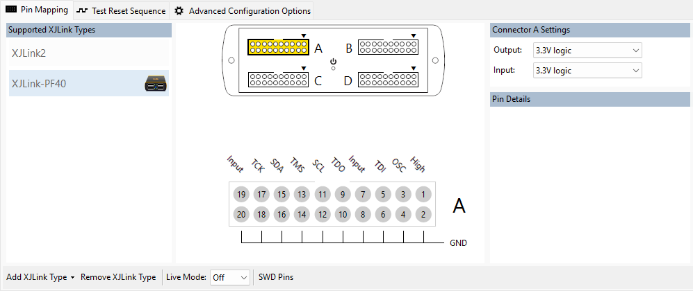
The toolbar under the graphical view of the pin mapping contains:
- Add XJLink Type - Allows you to add new types of XJLink to the Supported XJLink Types list. The specific type of XJLink can be chosen from the dropdown menu. Choosing FTDI opens the Add FTDI Details dialog.
- Edit FTDI Details - Opens the Edit FTDI Details dialog, which allows you to change the FTDI part, channel or netlist device used by an FTDI pin mapping. This button is only shown when an FTDI pin mapping is selected.
- Remove XJLink Type - Removes the currently selected XJLink type from the Supported XJLink Types list.
- Live Mode - Shows whether the XJLink is currently being accessed. If it is then the pin mapping will show the voltage read back for each pin. Live Mode can be enabled from the dropdown menu. Alternatively, it will be enabled when the JTAG Chain Debugger is being used.
- Use advanced settings - Enables advanced settings for the XJLink2 pin mapping, and is only visible when viewing an XJLink2 pin mapping.
- SWD Pins - Opens the SWD Pins dialog, which allows you to specify to SWDIO and SWDCLK pins required for SWD operations. Note that this option is not shown when viewing the XJLink2 pin mapping unless the Use advanced settings option is selected.
Pin Types
When customising the XJLink pin mapping, it is useful to have a safe starting point. The Load Pin Mapping Preset item on the Pin Mapping menu contains a Safe option which sets all pins to be inputs and is therefore a safe place to begin.
To create a custom pin mapping you need to define the behaviour of each pin required for connecting JTAG signals between the XJLink and the circuit under test. You can do this by right-clicking on a pin or selecting it and using the dropdown controls to the right, starting with the pin Type.
Many types of pins can be defined, such as PIO, High (drive high), Low (low output) and Input. Different types of XJLink can use different pin types - the hardware section for each type of XJLink explains all available pin types in full.
JTAG signals
The following pins must be defined in order to use JTAG:
- At least one Test Data Input to the circuit (from TDI, TDI2, etc). There should be one for each JTAG chain on the circuit being tested.
- Matching Test Data Outputs from the circuit (from TDO, TDO2, etc).
- At least one JTAG clock signal (from TCK, TCK2, etc).
- At least one JTAG Mode Select signal (from TMS, TMS2, etc).
TDI Driver Settings
Every TDI pin must have a TMS and TCK signal associated with it, and optionally an nTRST signal. This is referred to as a TAP. These settings only need to be changed from default when configuring dynamic chains.
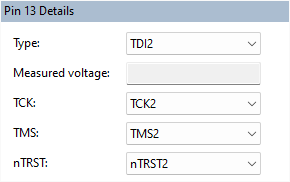
By default TDI pins are associated with the corresponding TMS and TCK signals (as well as the corresponding nTRST signal, if it is defined in the pin mapping).
When multiple TDI pins are used in a chain at runtime, all the associated TMS and TCK signals will be grouped together and driven as if they were a single TMS and TCK signal.
SWD Pins
SWD pins can be assigned via the SWD Pins button on the toolbar. Once assigned, they are denoted by a brown ring around the pin on the graphical representation. If a pin assigned as SWD is then defined as a Power pin in an XJLink2 pin mapping, a warning will be displayed and choosing Yes will remove both SWD assignments from the pin mapping.
XJLink types
The remaining options available to modify a pin mapping are different depending on the type of JTAG controller, and therefore are explained separately:
XJTAG v4.3.0