Configuring the XJIO board
The JTAG connection on the XJIO board is completely configurable. This means that it can work with any JTAG enabled board, irrespective of the pin mapping of the JTAG header on that board.
Configuring the JTAG connection
The configuration of the JTAG signals is done using jumpers JP1 to JP8.
In their default positions, the links on the configuration jumpers form a complete JTAG chain from the XJLink connector (CN1), through the JTAG chain on the XJIO board and back to CN1.
Not all of the links shipped with the XJIO board are required to form this chain; the following sections explain the purpose of each of the links needed to form the JTAG chain on the XJIO board and from there on to a board under test.
Signals coming from the XJLink
The XJLink is connected to the XJIO board using connector CN1. All of the configurable pins on the XJLink, pin 3 and pins 5 to 19, are then routed to jumpers where they can be linked to the appropriate signals for the JTAG chain of the XJIO board.
The pins of the jumpers are numbered to match the configurable pins of the XJLink. I.e. the numbering starts at 3, there is no pin 4 and then there are pins 5 to 19.
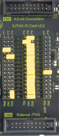
The JTAG Chain for the XJIO board
Each of the JTAG signals on the XJIO board is connected to one of the jumpers. The jumpers relating to TDI, TMS and TCK are positioned next to the jumpers connected to the XJLink connector, CN1. TDO works differently as the TDO from the XJIO board is the TDI to the Unit Under Test (UUT).
- Jumpers JP2 and JP5 are connected to the 16 user definable pins on CN1.
- Jumpers JP6 and JP8 are connected to the 16 user definable pins on CN2.
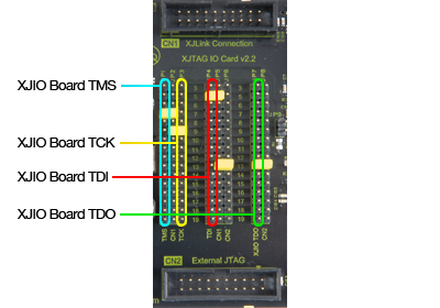
- Jumper JP1 is connected to the TMS input of the XJIO board.
- Jumper JP3 is connected to the TCK input of the XJIO board.
- Jumper JP4 is connected to the TDI input of the XJIO board.
- Jumper JP7 is connected to the TDO output of the XJIO board.
Placing links between JP5 and JP6 allows connection to be made between CN1 and CN2 to pass through any signals required, for example TMS and TCK to CN2 if an external JTAG connection is being used.
- TDI
- Placing a link between JP4 and JP5 allows the XJIO board TDI connection to be selected. If you are using the standard XJTAG pin mapping this link will be placed on the second pin down on JP5, which represents pin 5 on the XJLink.
- TMS
- Placing a link between JP1 and JP2 allows the XJIO board TMS connection to be selected. If you are using the standard XJTAG pin mapping this link will be placed on the fourth pin down on JP1, which represents pin 7 on the XJLink.
- TCK
- Placing a link between JP3 and JP2 allows the XJIO board TCK connection to be selected. If you are using the standard XJTAG pin mapping this link will be placed on the sixth pin down on JP3, which represents pin 9 on the XJLink.
Configuring TDO is done in a very similar way; however, this signal will normally come back to the XJLink via the board under test so two sets of jumpers are required to route the TDO signal. The first pair of jumpers, JP7 and JP8, route the TDO signal from the XJIO board to CN2. The second set of jumpers, JP5 and JP6, make the connection between CN2 and CN1.
The TDO signal from the last JTAG device on the XJIO board is connected to JP7. JP8 is connected to sixteen of the pins on the external JTAG connector CN2, pin 3 and pins 5 to 19. In order to route the TDO signal from the XJIO board to be the TDI signal on the board under test, place a link between the appropriate pins on these jumpers. To use the XJIO board without connecting to another board place the link on the tenth pin down on jumpers JP7 and JP8, which represents pin 13 on the external connector.
To complete the JTAG chain you will need to make a connection between the TDO pin on the external connector and the TDO pin on the XJLink connector. Placing a link between JP5 and JP6 will complete the JTAG chain back to the XJLink. To use the XJIO board without connecting to another board place a link on the tenth pin down on JP5 and JP6, which represents pin 13 on the XJLink.
Extending the JTAG chain
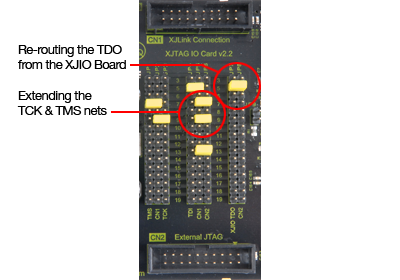
In almost all circumstances the JTAG chain on XJIO board will need to be linked to the JTAG chain on a board under test. Fortunately there is very little extra configuration that needs to be done to achieve this; the TDI signal will remain the same because the start of that chain is still the first device on the XJIO board.
The TMS and TCK nets need to be extended to include the appropriate pins on the external connector. This is done by connecting more links between JP5 and JP6. With the standard XJTAG pin mapping these links need to be placed on the fourth and sixth pins down across JP5 and JP6. These links match the positions of those that were placed to configure the TCK and TMS signals.
The TDO signal is once again slightly different. The TDO from the XJIO board now needs to be connected to the TDI of the external connector, therefore you need to move the link on JP7 and JP8 to connect the appropriate pins. If the XJTAG pin mapping is being used, the link will be placed between the second pin down. This will reconfigure the external connector to send the TDO from the XJIO board out as TDI, pin 5, of the external connector.
JTAG chain Termination
When the JTAG chain has been extended it may be necessary to terminate the TCK signal to prevent glitches. Placing a link on jumper JP9 will add a 120 Ω termination to ground.
Additional signals
If there is a requirement to be able to pass additional user defined signals - such as nTRST - through the XJIO board, further connections across jumpers JP5 and JP6 can be made.
Standard configurations
The table below lists the jumper connections required for the standard pin mappings supported by XJTAG.
| Pin Mapping | Default links | Link Modifications for External JTAG | ||||||
|---|---|---|---|---|---|---|---|---|
| TMS | TCK | TDI | TDO | TMS | TCK | TDO | nTRST/nSRST | |
| XJTAG | JP1.7 to JP2.7 |
JP3.9 to JP2.9 |
JP4.5 to JP5.5 |
JP7.13 to JP8.13 & JP5.13 to JP6.13 |
JP5.7 to JP6.7 |
JP5.9 to JP6.9 |
Remove JP7.13 to JP8.13. Place JP7.5 to JP8.5 |
- |
| Multi-ICE | JP1.7 to JP2.7 |
JP3.9 to JP2.9 |
JP4.5 to JP5.5 |
JP7.13 to JP8.13 & JP5.13 to JP6.13 |
JP5.7 to JP6.7 |
JP5.9 to JP6.9 |
Remove JP7.13 to JP8.13. Place JP7.5 to JP8.5 |
JP5.3 to JP6.3 JP5.15 to JP6.15 |
| Byte Blaster |
JP1.15 to JP2.15 |
JP3.11 to JP2.11 |
JP4.19 to JP5.19 |
JP7.13 to JP8.13 & JP5.13 to JP6.13 |
JP5.15 to JP6.15 |
JP5.11 to JP6.11 |
Remove JP7.13 to JP8.13. Place JP7.19 to JP8.19 |
-- |
| XJTAG Xilinx Adapter | JP1.7 to JP2.7 |
JP3.9 to JP2.9 |
JP4.13 to JP5.13 |
JP7.11 to JP8.11 & JP5.11 to JP6.11 |
JP5.7 to JP6.7 |
JP5.9 to JP6.9 |
Remove JP7.11 to JP8.11. Place JP7.13 to JP8.13 |
JP5.5 to JP6.5 |
XJTAG v4.3.0