Pin Mapping
This panel allows the circuit's JTAG connector to be configured.
XJTAG has several common connector mappings available as presets - these are the default XJTAG pin mapping, and those used by Multi-ICE, ByteBlaster and Xilinx. These can be selected via the Load Preset button. If none of these are appropriate for the circuit, the pin mapping can be customised.
Existing pin map files from previous projects can be loaded using the Load button.
XJLink2 Pin Mapping
Using the Load Preset button, select the "Safe" option. This sets all pins to be inputs and is therefore a safe place to begin the customised configuration. From this starting point, select each pin which is required for connecting JTAG signals between the XJLink and the circuit under test, and then either right-click or use the drop-down controls to the right to define their behaviour.
The following pins MUST be defined:
- At least one Test Data Input to the circuit (from TDI, TDI2, TDI3 or TDI4). There should be one for each JTAG chain on the circuit being tested.
- Matching Test Data Outputs from the circuit (from TDO, TDO2, TDO3 or TDO4).
- At least one JTAG clock signal (TCK, TCK2, TCK3, or TCK4).
- At least one JTAG Mode Select signal (TMS, TMS2, TMS3, or TMS4).
If your circuit requires other pins to be configured, then they can either be set as a constant value of High, Low (i.e. drive high or low output), Soft GND, or Input. They can also be set as: PIO, VREF1, VREF2, Run Button, Tests Running, Tests Passed, Tests Failed.
PIO pins
PIO pins can be used in a Test Reset Sequence to allow any particular sequences to be driven on the XJLink connector in order to set up the circuit for JTAG testing. They can also be driven and read from XJEase code.
VREF pins
If a VREF pin is assigned, the respective bank output voltage (see Advanced settings) is set to the voltage read from this pin. VREF1 sets the output voltage for bank 1, VREF2 sets the output voltage for bank 2.
If VREF pins are specified, their voltages are sampled and applied to the XJLink bank(s) under the following circumstances:
- Starting testing
- Enabling live mode on the Pin Mapping screen
- Running Get Max TCK, Check Chain or Signal Integrity scans
- Making particular changes to the Pin Mapping when Live mode is enabled - for instance changing which pin is used as VREF
Run Button
This is used to extend the Run Button input on the XJLink2 to work with an external push-button or other trigger. In this case, the pin on the XJLink2 should normally be held low; testing will start when the pin voltage is set high. The threshold at which tests will start can be altered when the Use advanced settings checkbox is enabled.
Tests Running/Passed/Failed
These can be used to indicate whether a test run is in progress, has passed or has failed. This allows the status to be displayed on external equipment. The pin is set High when the LED on the XJLink is illuminated to show that status.
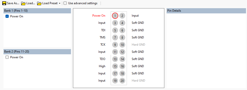
Bank Settings
The XJLink2 connector is split into 2 banks: Bank 1 (pins 1 to 10), Bank 2 (pins 11 to 20). The settings for Bank 1 can be modified in the "Bank 1 (Pins 1-10)" panel on the top left. The settings for Bank 2 can be modified in the "Bank 2 (Pins 11-20)" panel on the bottom left.
Bank Power Options
Power can be supplied to the hardware in one of two ways:
- Via an external power supply
- By the XJLink via the USB connection
The power is "Off" by default, which means the hardware expects to be powered by an external power supply.
USB power can be applied via Pin1 for Bank 1 by selecting "Power On" from the "Power" combo box in the "Bank 1 settings panel" or by double clicking Pin 1 on the visual representation of the XJLink.
USB power can be applied via Pin11 for Bank 2 by selecting "Power On" from the "Power" combo box in the "Bank 2 settings panel" or by double clicking Pin 11 on the visual representation of the XJLink.
It should be noted that applying power to a board that is already powered externally may damage your hardware.
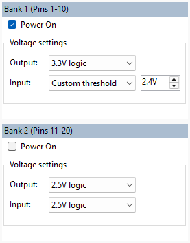
Bank Voltage Options
These options are only visible when the "Advanced Settings" checkbox is checked.
The voltage logic level for output pins can be set on a per bank basis. The voltage for output pins in bank 1 can be set to a preset value via the "Output Voltage" combo box in the "Bank 1 settings panel". The voltage for output pins in bank 2 can be set to a preset value via the "Output Voltage" combo box in the "Bank 2 settings panel". There are also custom values available if choose "Custom" in the respective combo box.
The custom voltage threshold for input pins can be set on a per bank basis. Note that each input pin can have an input voltage threshold corresponding to the custom value on its respective bank, or one of the preset voltages on a per pin basis. The voltage threshold for input pins in bank 1 can correspond to a preset logic level via the "Input voltage threshold" combo box in the "Bank 1 settings panel". The voltage threshold for input pins in bank 2 can be set to a preset logic level via the "Input voltage threshold" combo box in the "Bank 2 settings panel". There are also custom thresholds available if "Custom" is selected in the respective combo box.
Advanced Pin Settings
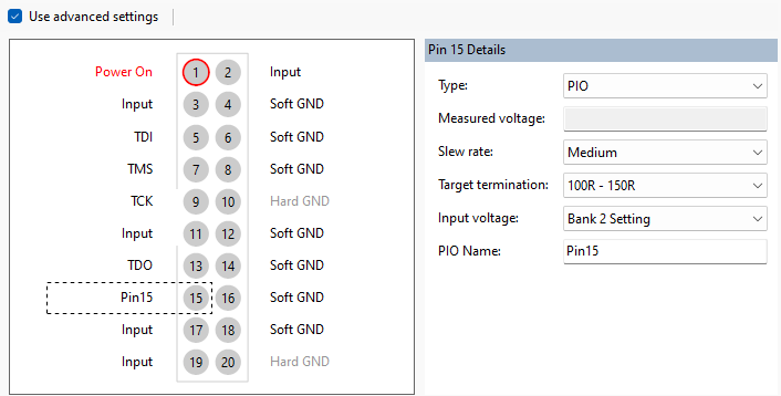
These options are only visible when the "Advanced Settings" checkbox is checked.
Slew Rate
The Slew rate for an output pin can be set to "Fast", "Medium" or "Slow". In general, this will not need to be altered.
Target Termination
Specifying the termination of the signal will allow an appropriate drive strength to be selected automatically.
Input Voltage
The input voltage for an input pin can be set to be the custom value on its respective bank (see Bank Voltage Options) or one of the preset logic levels.
XJTAG v4.3.0