Pin Mapping
XJTAG's XJLink controllers allow their connectors to be configured, and that must be done before the controller can communicate with the board under test. Any pin apart from the fixed GND pins can be allocated to a JTAG signal or to another input or output function. In this section of the user guide, we shall deal just with those aspects of pin mapping required to get the JTAG chain working.
This chapter describes how to assign the JTAG signals to the connector pins and the descriptions here can be used in many of XJTAG's applications.
- The Pin Mapping screen can be found in the following locations:
- XJAnalyser: click Edit JTAG Chain to launch the Project Setup.
- JTAG Chain Debugger: go to the Pin Mapping tab.
- XJDeveloper: go to the Pin Mapping screen.
- XJInvestigator: go to the Pin Mapping screen.
Common Pin Mappings
There are several preset pin allocations built into the software, and these can be loaded via Pin Mapping > Load Preset in the XJDeveloper or XJInvestigator menus, or the Load Preset button in XJAnalyser and JTAG Chain Debugger. These assign signals based on the standard connector pin-outs used by different manufacturers such as XJTAG, ARM and Altera/Intel.
The available preset configurations depend on the type of XJLink you are using.
If there is no preset configuration that meets your needs, a custom pin mapping will need to be created. Selecting the Safe mapping will set all pins as inputs and is the recommended starting point for any customised configuration.
JTAG Pin Allocations
The following pins are required for a JTAG interface:
- Test Data Input (TDI)
- Test Data Output (TDO)
- Test Clock (TCK)
- Test Mode Select (TMS)
There is also an optional 5th pin:
- Test Reset (nTRST)
Pins are assigned within the Pin Mapping screen by right-clicking on each pin number and selecting the required function, or by left-clicking the pin number and editing its type in the Pin Details pane.
Some devices have the optional asynchronous reset (nTRST) signal in addition to the 4 mandatory JTAG signals. Although this is optional, if your device has an nTRST signal it should be connected to the XJLink, and the XJLink pin assigned the required function.
Associating Signals with TDI
Because the XJLink2 supports multiple TAPs simultaneously, there are multiple data inputs (TDI, TDI2...), data outputs (TDO, TDO2...), clocks (TCK, TCK2...) Mode Select signals (TMS, TMS2...) and reset signals (nTRST, nTRST2...).
The relationship between data inputs and outputs is fixed (ie. TDI is always linked with TDO; TDI2 is always linked with TDO2 etc.), but the association of each TDI signal with particular Test Clock, Test Mode Select and Test Reset signals is configurable to match the hardware under test. It is therefore necessary to tell the software which TCK, TMS and nTRST signals to associate with each TDI; this is done as part of assigning TDI to a pin.
- The same TCK, TMS and/or nTRST signals can be used with multiple TDIs (eg. TDI2 and TDI3 could both use TCK2)
- The set of TDI, TDO, TCK and TMS signals that are used together, along with any nTRST pin used with them, is known as a TAP Group
The TDI pin is grouped with its associated TCK, TMS and nTRST signals in the Pin Details pane:
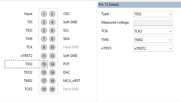
Figure 8: Associating TCK, TMS and nTRST with a TDI pin
- For clarity and project maintainability it is normal to use TDI with TMS and TCK; and for TDI2 to form a group with TMS2 and TCK2 etc. Likewise it is usual to group nTRST with TDI, and nTRST2 with TDI2 etc.
Profiles and Dynamic Chains
If more than one JTAG chain is being used and they have different sets of TCK and TMS signals, profiles can be defined to determine which chain runs at a particular point. This type of chain is called a dynamic chain and removes the need for all chains to run simultaneously. The most common scenarios where this may be useful are:
- Power control: if one JTAG device controls the power for others, it is necessary to get that chain running first before the rest of the chain can be accessed.
- Programming: when using JTAG for programming, dynamic chains may reduce programming time.
- Faster testing: on some boards, dynamic chains can allow tests to run faster.
- Easier debugging: when debugging problems with a long JTAG chain, it can be advantageous to temporarily reduce the number of devices in the chain.
- Profiles can be defined or edited by selecting the Advanced Configuration Options tab, on XJDeveloper's Pin Mapping screen.
Programmable IO (PIO) pins
In addition to the JTAG signal types, you can set pins on an XJLink to be PIO pins. These can be used for general-purpose testing, but PIO pins can also be used in Test Reset Sequences. This functionality is often needed in order to put JTAG-compliant devices on the UUT into the correct mode for JTAG testing.
An example would be that you might use a PIO pin to control the power supply to a JTAG device. The Test Reset Sequence would therefore first set the power supply's enable signal, then wait for a suitable period before doing any necessary manipulation of the JTAG TAP signals.
When a pin is defined to be a PIO pin, its name can also be changed to something descriptive:
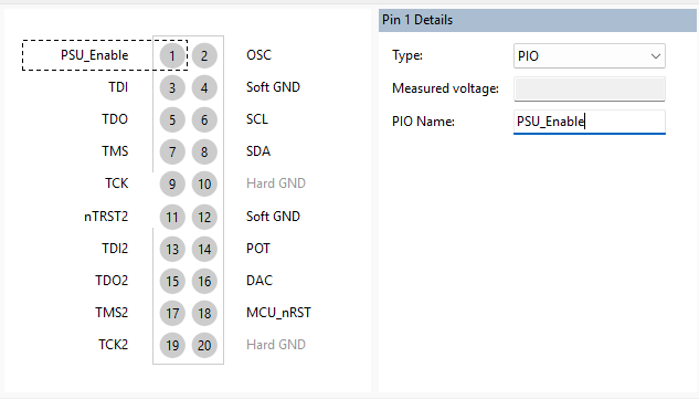
Figure 9: Changing a PIO pin name
Ground Pins
The XJLink2 connector has two fixed grounds on pins 10 and 20. In addition, other pins can be given the Pin Type Soft GND. A soft ground is a pin that is connected to ground through a FET. It is not as good as a hard ground but provides a relatively low impedance path.
XJLink-PF series controllers have 10 ground pins (pins 2, 4, 6, 8 & 10) on each connector. Any connector with TAP or PIO pins configured should have a physical GND link to the UUT.
Please refer to A Guide to JTAG Grounding and A Guide to JTAG Pin-out for details of how best to use these ground connections.
Bank Settings
The XJLink2's connector is split into two banks (pins 1 - 10; and pins 11 - 20), which can operate at different voltage levels. For each bank, the input and output voltage ranges can either be selected from the standard supply voltages of 1.2, 1.5, 1.8, 2.5 and 3.3 V or set to customised levels; the default setting is 3.3 V logic compatibility.
For XJLink-PF series controllers, there is a voltage bank per connector – each connector can operate at a different voltage level.
The bank voltages are chosen from dropdown menus on the Pin Mapping screen. For an XJLink2 you must tick the Use advanced settings box to make these settings visible:
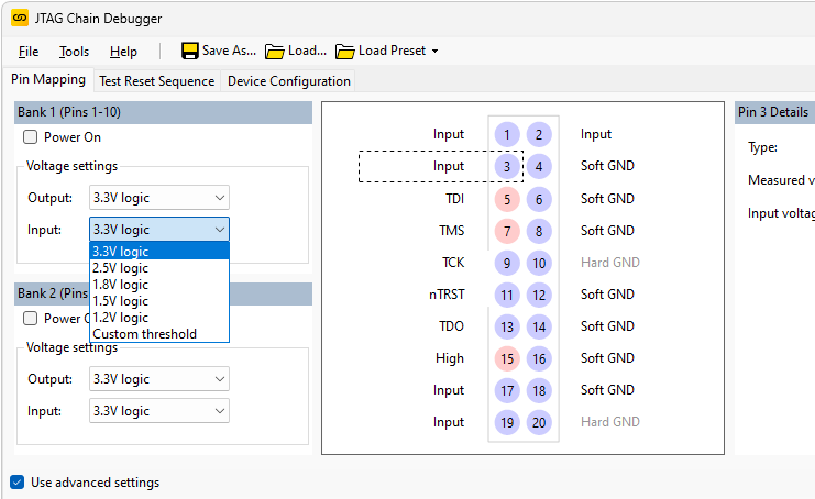
Figure 10: Setting a Bank Voltage
- When the customised voltage setting is chosen for an input, you are setting its voltage threshold, not its logic level.
Once a bank voltage has been selected, all the pins in that bank will be set to the chosen logic levels. However, it is still possible to modify specific input pins in that bank (eg. TDO or a PIO) to work with different input voltages: in the Pin Details pane, the input voltage range can be changed from its default bank setting to an alternative standard logic level:
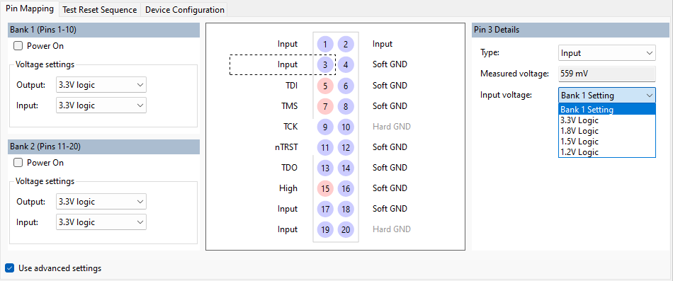
Figure 11: Exceptions to bank voltages
This can be useful when level shifters have been used on the UUT and its outputs are at different logic levels to its inputs.
- The Power on box (only available for XJLink2-series controllers) is normally left unticked. If selected, the XJLink2 will attempt to power the UUT via its connector (pin 1 from bank 1 and pin 11 from bank 2), which may cause damage because it only has very low output current capability.
Output Driver Settings
If you are using an XJLink2 and have the Use advanced settings box ticked, you can adjust an output pin's slew rate and target termination. These will be used later if necessary for optimisation of signal integrity, but at this stage should be left at their default settings.
See the section on Adjusting Slew & Target Termination for more details.
XJTAG v4.3.0