Examples of Device Categorisation
This section describes how to categorise some common circuit blocks where the choice of category for the devices isn't obvious. The following examples are used to explain the factors that will influence your decision on which categories to choose:
- FET power rail switch
- Regulators
- When to categorise logic as Passive
- Clock buffers
- Bidirectional switches
- Watchdog devices
Other examples have already been covered elsewhere in this user guide:
Categorising Devices that Control Power
When deciding how to categorise devices that control power rails, it is important to consider how testing will be impacted if they are switched on and off. For example, if a transistor powers an important part of the circuit (such as a JTAG IC, devices that will be tested, or accessible pull-ups), the categorisation process should ensure the voltage output will not switch off during the connection test. If the voltage rail being considered provides the input to any other regulators, it will also be necessary to check the impact on circuitry powered by those additional regulators.
It is also important to note that allowing Connection Test to drive nets that control power will result in those voltage rails turning on and off many times in rapid succession (possibly at around 10 kHz). If that will cause a problem, the categorisation process must ensure any relevant control lines are held at fixed states during the connection test (some regulators may be negatively affected by continuous switching, especially if it causes repeated bursts of inrush current).
How to deal with these considerations during categorisation is described with two examples below – a FET power switch and a regulator.
Categorising a FET Power Switch
Consider the FET power switch of Figure 54:
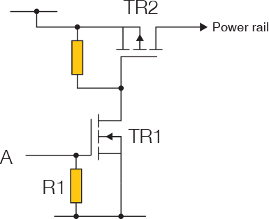
Figure 54: P-Channel MOSFET Power Switch
To be able to test TR1, there must be access to its gate (A) and there must be a way to confirm the power rail has been switched. If those are not possible, the transistors cannot be tested (other than possibly checking TR1's gate for shorts and stuck-at faults as part of the connection test). In that situation, TR1 can be categorised as Ignored.
- Explorer provides an easy way to determine if it is possible to control TR1's gate.
It may be desirable to stop the power rail switching on and off during the connection test by holding TR1's gate at a fixed level. However, the impact of doing so on test coverage must be considered: with the output kept on, Connection Test can check devices connected to the output power rail such as pull-resistors but will be unable to check R1 on the gate. Alternatively, if the gate is not held at a fixed value, Connection Test can check R1 but will be unable to test pull resistors connected to the output supply rail because the power will be switching on and off during testing. Which situation gives the best test coverage therefore needs to be considered when deciding which approach to take.
When a Power Rail Must be Fixed During the Connection Test
The power rail can be kept continuously active or inactive for the duration of the connection test when TR1 is categorised as either Test or Ignored. Which categorisation to choose will depend on whether the circuit block can be tested using XJEase.
If it's possible to detect the impact of the circuit being switched, it's often best to hold TR1's gate fixed during the connection test, and then to use an XJEase test to switch the rail and to monitor the effect (e.g. by checking a pull-resistor connected to the supply). In that situation, TR1 should be categorised as a Test device.
There are two methods for keeping the power rail in a fixed state during the connection test:
- If TR1 is categorised as Test, you can either apply a Disable value of High to its gate pin using its test device file, or set a Constant pin on XJDeveloper's Constant Pins screen.
- If TR1 is categorised as Ignored, you can set its gate as a Constant pin on XJDeveloper's Constant Pins screen.
- Explorer can be used to see if the gate will be prevented from switching during the connection test by a Constant pin or by another device in the circuit imposing a Disable value on the net. Rather than having to examine each test device individually to check for Disable values, using Explorer provides a summary view of all Disable values and Constant pins being applied to the net, and therefore shows if anything is stopping Connection Test checking TR1.
The best approach for fixing the gate value depends on whether the same circuit configuration is used elsewhere on the board. If switched power rails are used in several places and they all need to be kept in the same state, it is likely to be more efficient to create a test device file and to use it for each transistor, rather than setting multiple Constant pins. However, if one of the following situations apply, it is normally easier to control the gates using Constant pins:
- The switching circuit only appears once on the board.
- The switching circuit is reused elsewhere, but the other instances don't need the transistors to be held in the same state – for example, because they provide power rails that need to be kept in different states, or the circuit is reused for a different function (such as controlling an LED rather than a power rail).
Constant pins and Disable values can both be overridden during XJEase testing.
In the circuit of Figure 54 above, a test on TR1 may also be able to check R1 for open circuits. Provided the output supply rail decays fast enough after being switched off, a test could be written that turns TR1 on and checks the power rail is present; and then sets the JTAG pin driving the gate to high impedance and confirms the pull-down effect of R1 has switched power off.
If the transistor isn't going to be tested and there's no requirement to set a Disable value, it should be categorised as Ignored instead of as a test device.
When the Power Rail is Not Fixed During the Connection Test
In circuits where it doesn't matter if the output power rail switches on and off during the connection test (e.g. because it only goes to a connector pin that has nothing attached), there is no need to hold TR1's gate constant. In that case, Connection Test can be allowed to drive the net connected to the gate, and TR1 can therefore be categorised as Ignored if it's not going to be tested with XJEase.
If the circuit block can be tested (e.g. if there is an LED on the power rail that can be monitored), an XJEase test should be used as described in When a Power Rail Must be Fixed During the Connection Test above.
- Allowing the transistor to be controlled during the connection test will result in the power rail being rapidly switched on and off many times. This may be undesirable, in which case a Disable value or Constant pin should be used to hold it in one state.
Categorising Regulators
The next step up in complexity from a FET switch is a regulator that can be turned on via an Enable pin. When deciding how to categorise a regulator, the same considerations of access and whether to allow it to switch during the connection test apply as they do for the FET power switch described above, so that section should be read before continuing.
A difference to the FET switch is that a regulator may have a PowerGood output, which can mean it is best to categorise it as Test.
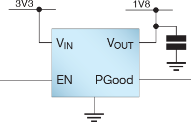
Figure 55: Regulator with a PowerGood Output and Enable
If there is boundary scan access to the PowerGood and/or Enable pins, you may be able to check those pins, depending on the behaviour of the PowerGood output.
It is only possible to test the PowerGood pin for open circuits if circumstances can be generated that cause the regulator to drive the pin. However, many regulators have an open-collector or open-drain PowerGood output and rely on an external pull-up to indicate a valid output voltage, only driving the pin when a fault condition is detected while the supply is enabled. In a test, the Enable pin could be used to switch off the output, but that will only cause the PowerGood output to be driven if the signal still functions with the regulator disabled, which is not the case for all regulators. If the conditions can be met that make the regulator drive its PowerGood pin, it can be categorised as a test device.
To test the PowerGood output in that way, you will need to create an XJEase test device file.
When to Categorise Logic as Passive
When the speed of the test is important, and a block of logic is complex (e.g. several cascaded gates), it may be appropriate to categorise some of that logic as passive devices, as explained above in the Logic Category section.
For example, consider a non-inverting buffer: the only difference to a series resistor in terms of how the digital value passes through it is that the signal path is unidirectional instead of bidirectional. However, in some circuit configurations, the signal flow through a series resistor may also only ever be unidirectional, such as when it's in the MOSI signal path of a SPI bus. In those situations, it can be appropriate to categorise a logic gate as Passive. Compare the signal flow in the two circuits of Figure 56. In the upper circuit, a buffer, IC3, connects a JTAG device to the input pin of a non-JTAG device. During boundary scan testing, the signal direction in the upper circuit can only be from IC1 to IC2. Similarly, in the bottom circuit, because the pin on IC2 is an input, the signal flow can only be from left to right, towards the non-JTAG device's input pin. Because the behaviour is the same for both circuits, it is valid to categorise IC3 as if it was a passive device as part of the process of simplifying complex logic.
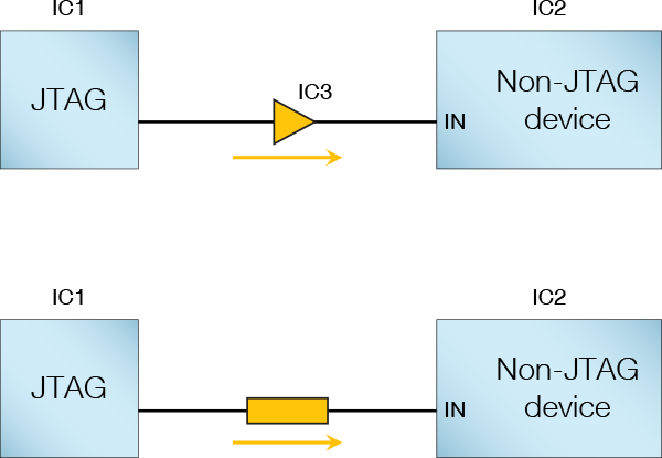
Figure 56: In Some Cases, a Logic Device can be Categorised as Passive Connect
- When a logic device is categorised as Passive, the access shown in Explorer will be incorrect because it will be based on the device being passive and will think that IC1 can read IC2's input pin.
Examples of when and how to do this are illustrated below when the categorisation of a voltage translating switch and a clock buffer are considered.
One situation when a logic gate must be categorised as Passive is when it forms part of the JTAG chain. XJTAG does not support devices categorised as Logic in that part of the circuit, and those logic gates must therefore be categorised as Passive. This is acceptable because the signal path in the JTAG chain is always unidirectional, and Connection Test will never interact with any nets in the JTAG chain (because doing so would stop the chain working).
Categorising logic in the JTAG chain is performed as part of defining JTAG chains rather than on XJDeveloper's Categorise Devices screen.
Categorising Clock Buffers
Consider the example of Figure 57 below, which comes from the XJDemo v4 board. The clock buffer U15 could be categorised as Passive, Test, or Logic, and it would still be possible to confirm the clock is running. The following sections will explain the impact on test coverage of these alternative categorisations. In each case, U9 will be categorised as Logic, irrespective of what is chosen for U15.
Connection Test will not test this circuit block in any of the approaches described below because, whatever categorisation is used, an uncontrollable non-JTAG device will always be driving the three clock nets, and so Connection Test will be unable to control them. All three approaches therefore require an XJEase test to be run for this circuit to be tested.
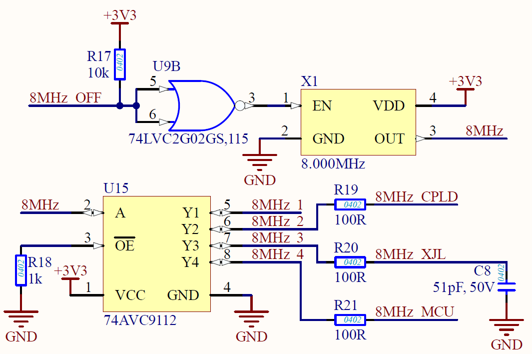
Figure 57: Example Clock and Clock Buffer Circuit
Categorising U15 as Passive
The clock buffer U15 could be categorised as Passive. The circuit is then tested by categorising the X1 oscillator as Test with the standard XJTAG library file (XTAL_OSC.xje) and using its Test()() function.
To categorise U15, create a new Passive Device file with connections between the buffer's input pin and each of its outputs as shown in Figure 58 below.
Because it's now considered to be a passive device, it's important to ensure the system knows it cannot drive back through it to the oscillator and to the other output nets. This needs to be done by placing a Disable value of Excluded on the oscillator's output (which restricts everything connected to that net to be an input only). In this case, if the library file is used, setting this Disable value will happen automatically because it is already included in the test device file.
The effect of U15 being categorised as Passive is that this disable value will be applied through the circuit to the 8MHz_CPLD, 8MHz_XJL, and 8MHz_MCU nets. Connection test will therefore not test any of this circuit, and all testing will be done using X1's test device file.
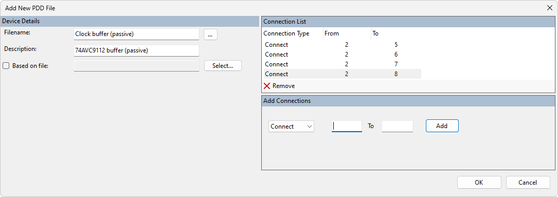
Figure 58: Creating a Passive Device File for a Clock Buffer
The standard XJEase library file used for the oscillator will allow the clock output(s) to be checked. However, in a circuit like Figure 57 above where there are several points at which the clock can be accessed, the XJTAG system will automatically select one of the outputs for the test, which will leave the other outputs untested. To get good test coverage, the test should therefore be run three times, with it forced to use a different net each time. For details of how to change a test's settings so that it uses a particular net, refer to the user guide on Setting up a Test List.
The advantage of this approach is that no additional XJEase code needs to be written. However, the disadvantage is that test time will be increased because the oscillator test will need to run multiple times.
Categorising U15 as a Test Device
By categorising U15 as a test device, it is possible to check all three outputs simultaneously. This approach will therefore give the best test time but has the disadvantage that some additional XJEase code is required.
A test device file will be required for U15, but it can use the test functions from the library's additional code file, Oscillator.xje to check for level transitions on the outputs. The test for U15 should be run once to prove the clock is working and then be repeated with the oscillator disabled to confirm the clock then stops. To control the Enable pin on the oscillator, X1 should also be categorised as a test device, and a circuit code file written to control it as part of an overall test, calling the necessary functions from the test device file.
Because the clock signal will be present on the buffer's outputs during the connection test, it is important to prevent Connection Test from driving against them. The buffer's test device file therefore needs to set Disable values of Excluded on the buffer's output pins.
In addition, for the project to report the correct test coverage, it will be necessary to define U15's input and X1's output as functionally tested in the test device file's Busses section – see the user guide on Creating Test Device Files for details of how to do this.
Categorising U15 as Logic
Because the clock buffer U15 can be described by a truth table, it could alternatively be categorised as Logic, with X1 categorised as Test to provide the XJEase functions. The test method is then the same as when U15 is described as Passive, except, for this categorisation, there is no need to set a Disable value to prevent Connection Test driving the buffer's outputs because Connection Test already understands this for logic devices.
One advantage over categorising it as Passive is that there is no longer a risk of forgetting to add the Disable value or later accidentally changing it.
Categorising as Logic will also mean that the reported test coverage statistics are accurate because U15's Enable pin will be checked for stuck-high faults.
A small disadvantage of categorising the clock buffer circuit in this way is that test execution may be very slightly slower because the system will need to do more computations to work out the different logic combinations.
Categorising a Bidirectional Switch
How to categorise a bidirectional switch depends on what device(s) are connected to the switch, whether the signals are unidirectional or bidirectional, and what ability there is to control the switch. The circuit will be tested by the connection test and an XJEase test, and a key objective is to categorise the devices in a way that allows Connection Test to achieve the best shorts coverage. This will normally be supplemented by an XJEase test to check for open circuits.
This section describes how to categorise the devices in these situations:
- When the data flow through the switch is bidirectional, such as when a JTAG device connects to a QSPI peripheral through a simple voltage-translating switch.
- When the data flow through the switch is bidirectional, and the switch is used to connect a device to one of several JTAG devices.
- When a multiplexer connects a device to one of several JTAG devices, and the data flow through the multiplexer is always unidirectional.
- When an I2C Multiplexer connects a JTAG device to I2C devices on different output channels.
Simple Bidirectional FET Switch
Consider the circuit of Figure 59, where a voltage-translating bidirectional switch is used to interface a JTAG IC to a QSPI device.
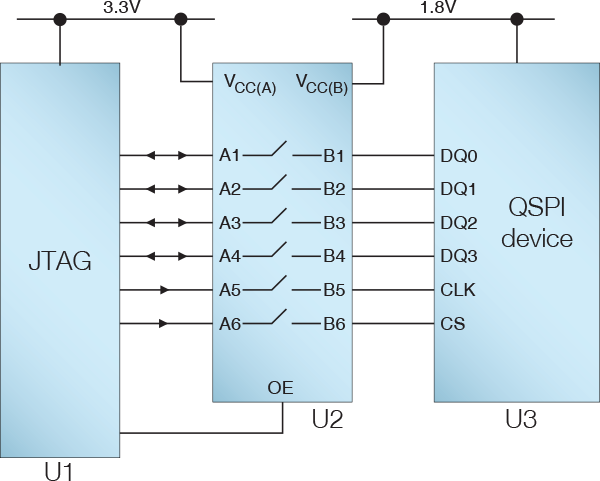
Figure 59: A Bidirectional Voltage Translating Switch
The simplest approach is to categorise U2 as Passive with a Connect between A and B for each switch, and to set a Constant pin on U2's Output Enable to keep the switches always closed. This will allow Connection Test to check for shorts on the JTAG device, all the A and B pins of U2, and the QSPI's six pins (although it will be unable to detect a short between associated A and B pins because the switch will be connecting them). U3 can be categorised as a Test device, with a function to check the pins for open circuits.
To categorise U1 from the Categorise Devices screen, assign it as Passive and click in the Assign Device as Passive dialog to create a new Passive Device file. This will open a dialog similar to Figure 60, in which you can define a connection type of Connect between A1 and B1.
Figure 60: Creating a Passive Device File for a Switch Categorised as Passive
Click and then repeat the process for the other A-B pairs. Once they have all been added, click to create the new PDD file.
Note that this approach results in no test coverage on U2's Output Enable because a Constant pin is needed to hold it in a fixed state to allow Connection Test to run correctly. For the Output Enable pin to be tested, U2 would need to be categorised as Logic, with a truth table that includes the pin. However, in that case, a test function cannot be run on the QSPI device because XJDeveloper would not understand how to read U3's data lines because connecting via a (unidirectional) logic device would prevent an output from U3 reaching the JTAG device.
This trade-off therefore needs to be considered: categorising U2 as Passive results in shorts and opens coverage on all six pins of the QSPI but gives no coverage of U2's Output Enable. Categorising U3 as Logic allows the Output Enable to be tested for shorts but loses opens coverage for the circuit. In this example, the best compromise is to accept the loss of coverage on the Output Enable.
Complex Combination of Bidirectional FET Switches
In the circuit of Figure 61 below, only one of the two switches can be enabled at a time.
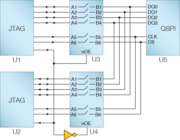
Figure 61: Two JTAG Devices Connected to a QSPI Memory
Because some of the signals through the switches are bidirectional, and the direction cannot be controlled during the connection test, the switches should not be categorised as Logic (which assumes a unidirectional data flow). If they were categorised as Logic, it would not be possible to run a test function on the QSPI device because the XJTAG system would not understand how to read U5's data pins.
Passive categorisation is more appropriate but it would be wrong to categorise both U3 and U4 in that way because Connection Test would then think there was a continuous path between U1 and U2 via the switches; it would therefore incorrectly flag errors during the test. To avoid this, only one switch should be categorised as Passive. In this example, we will choose U3 to categorise in that way.
So that the circuit's behaviour matches U3's categorisation as Passive, a Constant pin needs to be set on its Output Enable to keep its switches closed.
With U3 categorised as Passive, there will be test access to the QSPI device, U5. Categorising U5 as Test with a standard QSPI test device file from the XJEase library will then allow it to be tested using the path through U3.
The other switch can be categorised as Test. A new test device file will need to be created because, instead of categorising it like a switch, the technique is to categorise it as if it was the QSPI device. A copy of U5's test device file should be used, with the bus definitions modified so that the QSPI signals are mapped to the switch's A pins. When the test function is run and the system interacts with U4, it thinks it is accessing the pins of a QSPI device whereas, in reality, it is accessing the QSPI via U4.
U4's test function must also override the Constant pin to alter the state of the Output Enables so that its switches are closed when its test is running.
Testing will be completed in several stages:
- Check for shorts as part of the connection test. As with the previous example, this will check all pins except the two Output Enables, although it is unable to detect shorts between associated A and B pins on U3 because the switch will be connecting them.
- With the Constant pin still keeping U3's switches closed, run the library test function on U5 to check the upper half of the circuit for open circuits.
- Run U4's test function to check the lower half of the circuit for open circuits.
For details of how to categorise U3 as Passive, see the earlier example of a simple bidirectional FET switch.
For help creating a test device file for U4, follow the steps described in the user guide chapter on How to Create Your Own Test Device Files.
Simple Multiplexer With Unidirectional Data Flow
Consider the circuit of Figure 62 below, where two JTAG devices are connected to a SPI memory via a bidirectional switch. In this case, U3 cannot be categorised as Passive because that would necessitate defining a connection between A and D and also between B and D. Although that would allow XJEase tests to run on U4 to check the path from U1 and the path from U2, it would break the connection test because the switch does not physically connect in that way. (Categorising a switch as Passive was possible in the previous example because the two JTAG devices were connected via physically separate switches, allowing Passive categorisation to be restricted to a single route through the circuit.)
When deciding how to categorise these devices, it should be noted that all the signals are unidirectional: D2 on the switch is always acting as an input, and D1, D3, and D4 are always acting as outputs. If the test system has access to the switch's Select input, the switch U3 can be categorised as Logic because the signals are unidirectional.
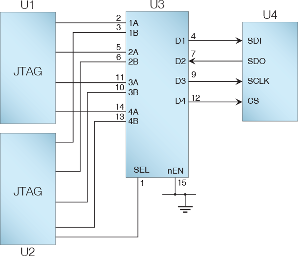
Figure 62: A Bidirectional Switch with Unidirectional Signals
The steps to create a new logic device for U3 in this circuit configuration are as follows:
- Categorise the device as Logic to create an entry in the Logic Device Descriptor file.
- Add a truth table for the situation when D is an output (for D1, D3, and D4).
- Add a second truth table for the situation when D is an input (for D2).
- Allocate the pins.
These steps are described in detail below.
Categorising U3 as Logic is only appropriate because the signals are unidirectional. If U4 was a QSPI device, for example, some data lines would be bi-directional, and an alternative approach would be necessary.
1. Create an Entry in the LDD File.
To create a new entry in the Logic Device Descriptor file during categorisation, assign the device as Logic and then click :
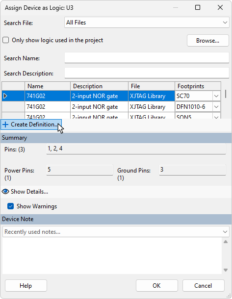
Figure 63: Creating a New Logic Definition During Categorisation
This opens the Add New Logic Device Definition dialog, in which you will need to provide a suitable name for the logic definition. In this example, the definition will be unique to this circuit, and a clear circuit-specific name such as U3 SPI MUX should therefore be used. The system also needs to know in which file to enter the new logic definition. This will normally be Local XJTAG Logic.ldd, which is automatically created the first time a Logic Device Definition file is used:
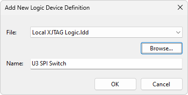
Figure 64: Creating a New Logic Device Definition
- If the logic definition can be re-used elsewhere, a generic name should be used that describes its function.
Click to create the entry, and you will be returned to the Assign Device as Logic dialog. Click to complete the assignment.
2. Create the First Truth Table
It is now necessary to create suitable truth tables for the individual gates in the multiplexer. As shown in Figure 65 below, right-click on the newly categorised device and select from the context menu to open the logic definition on the Logic Files screen. Click as shown:
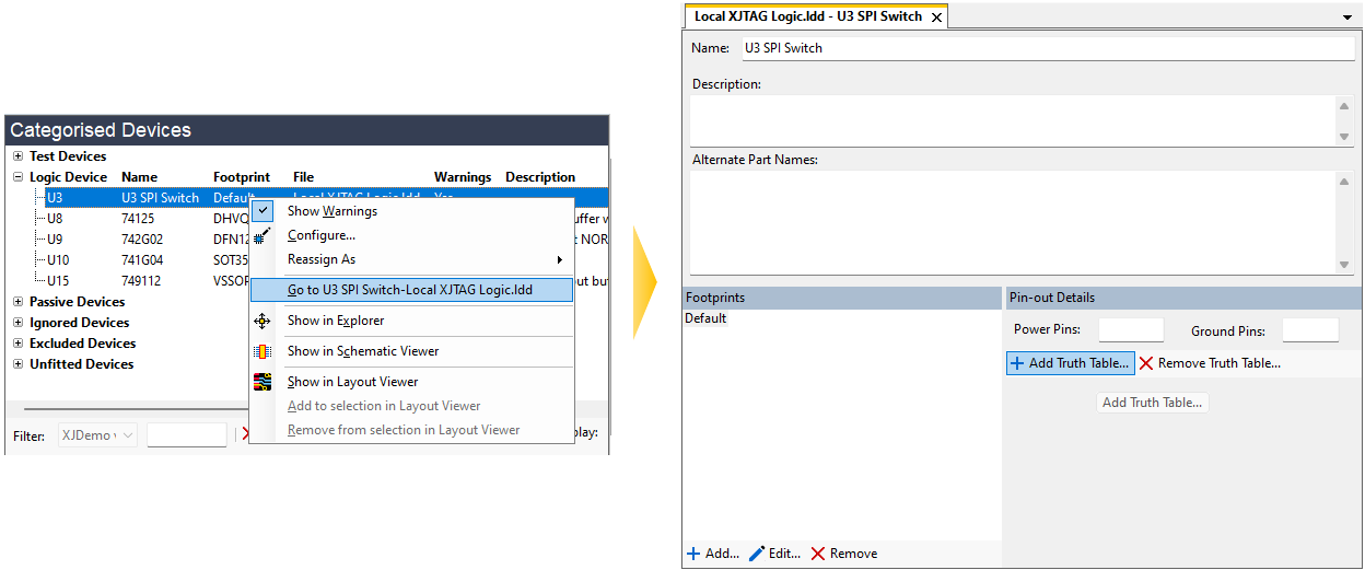
Figure 65: Adding a Truth Table to a Newly Created Logic Definition
You can now start creating the truth table (Figure 66 below). In this example, first create the table for the switches where D is an output: select the radio button and provide a name. It is best if this is generic to aid reuse: for example, 2 to 1 MUX.
Click , and you will be asked to provide the truth table's column headings in the Add Columns to Truth Table dialog. In this example, you will want four columns – three inputs (SEL, A, and B) and one output (D). Enter these headings separated with commas and click :
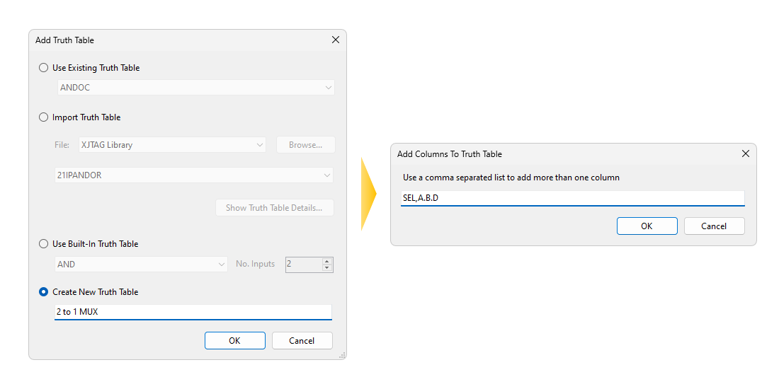
Figure 66 Defining Truth Table Column Headings
The next screen will allow you to enter data for the truth table (see Figure 67 below). Create the values by selecting the different logic states from the dropdown menus in each cell: inputs are represented by H, L, and X (don't care); and outputs by 1, 0, and Z (high-impedance).
- A guided exercise on creating truth tables can be found in the XJTAG Help system.
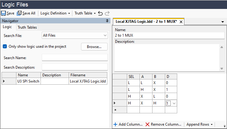
Figure 67: Adding a New Truth Table
Enter a reminder of what the truth table is for in the Description box and click .
3. Create the Second Truth Table
The second truth table can now be created as shown in Figure 68 below to deal with the switch that uses D as an input: select the tab that has the logic device definition and then click again.
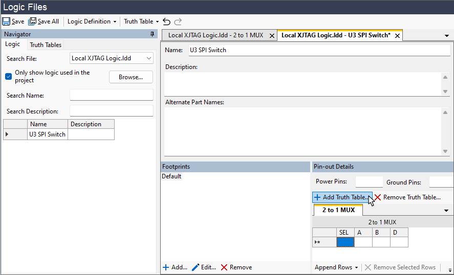
Figure 68: Adding a Second Truth Table
Repeat the process used for the first truth table to create a new one for when D is the input. Provide a generic name for the truth table such as 1 to 2 DMUX:
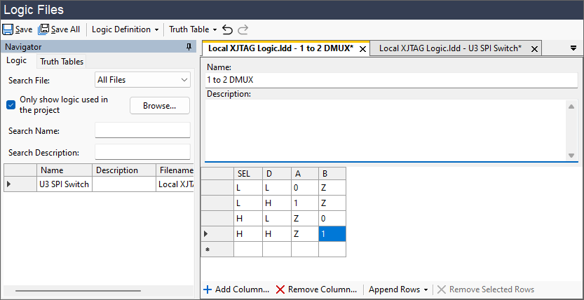
Figure 69: Creating the 2nd Truth Table
When pin A or B are not internally connected to D, they will be high impedance, so the Z entry is used for them as shown in the figure above.
Once the new truth table has been created, click  Save (you cannot use
  Save All at this point because the logic device definition is incomplete).
4. Allocate the Pins
With both truth tables added, the next stage is to provide the device's pin-out as shown in Figure 70 below. In the tab for the Logic Device file, provide a description and type the pin numbers directly into the cells. To switch between its two truth tables, select the relevant tab:
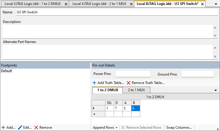
Figure 70: Adding Logic Device Pin Numbers
For a device with the pin-out shown in Figure 62, the entries will be:
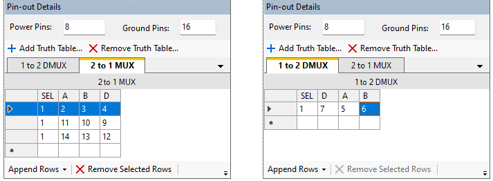
Figure 71: Entering Pin Numbers for Both Truth Tables
For completeness, the power and ground pin numbers can also be entered in their separate boxes. The entry in the Footprints box can be left as default.
In this example, the switch's Enable pin is directly connected to ground. It is therefore not used during testing and so does not need to be entered into the logic device's definition. If the Enable pin was being used, the signal would need to be included in the truth table, and the pin number would be required in the logic device definition. This also applies if the same logic device is used in multiple places on the board and any of them uses the Enable pin; this ensures a common device file is created.
Click Save All to save the new logic definition.
With U3 described as Logic, there is now boundary scan access to the memory, U4, which can then be categorised as Test, using the standard library file to provide the test function.
Categorising an I2C Multiplexer
In the example of Figure 72 below, an I2C multiplexer is controlled by writing to its internal register. Once a particular switch output has been selected, the downstream peripherals on that channel can be accessed over the bus.
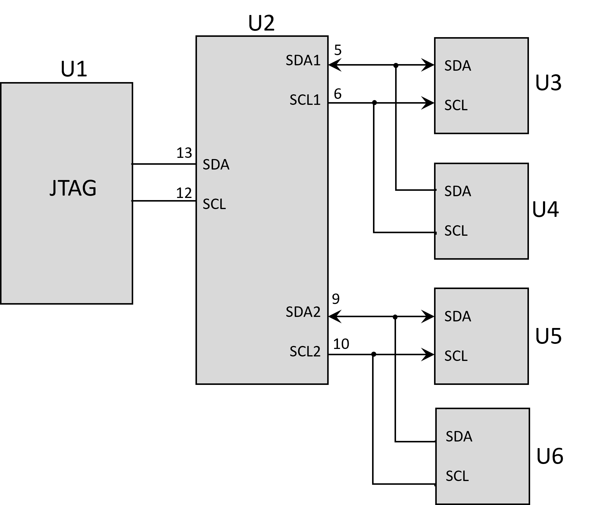
Figure 72: An I2C Multiplexer
Because U2 needs to be controlled over the I2C bus to switch between its outputs, it must be categorised as Test. A suitable test device file should be available in the XJTAG library, but if a different one is required, it can be created as described in Creating Test Device Files, with test functions copied from a similar library file. U2's test device file will need to include a function to switch between the multiplexer's outputs.
The I2C peripherals are also categorised as Test, using test device files relevant to those devices.
Because test functions will be run on the four I2C peripherals, XJDeveloper needs to know it has access to them through the multiplexer. Categorising U2 as Test does not do this, so connections must be manually added into the project that link U2's SDA and SCL pins to corresponding pins on the other side of the switches. To do this, go to the Connections screen and click  Add Connection... to open the dialog shown in Figure 73:
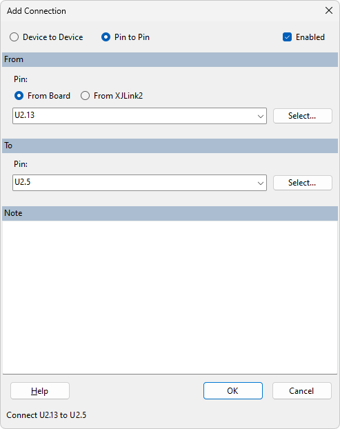
Figure 73: Telling XJDeveloper it has Access to Downstream Devices
Select the connection type of and choose . Type the pin number for U2's SDA pin (pin 13) directly into the From box in the form <reference designator>.<number>. If your project has multiple boards, it should be prefixed with the board name (e.g. mainboard.IC2.13).
- As an alternative to typing the pin number directly into the box, you can click to open the Device and Pin Selector, and pick the pin from there.
To define the link through the multiplexer to its first downstream port, type the pin number for U2's SDA1 pin (pin 5) into the box in the To area. Click to enter the connection.
Repeat the above steps until the following connections have been defined:
| From | To |
|---|---|
| U2 SDA (U2.13) | U2 SDA1 (U2.5) |
| U2 SDA (U2.13) | U2 SDA2 (U2.9) |
| U2 SCL (U2.12) | U2 SCL1 (U2.6) |
| U2 SCL (U2.12) | U2 SCL2 (U2.10) |
Once they are all entered, click .
With U2 – U6 all categorised as Test, it is best to create a circuit code file that performs the following steps:
- Run a function from the multiplexer's test device file to select SDA1 and SCL1 as the output.
- Run a test function from U3's test device file (e.g. a basic address acknowledgment) to test the route through the SDA1 and SCL1 pins. It is likely to be most efficient to then also run a test on U4 while the multiplexer is switched to that output.
- Run a function from the multiplexer's test device file to select SDA2 and SCL2 as the output.
- Run a test function from U5's test device file to check the route through the SDA2 and SCL2 pins. It is likely to be most efficient to then also run a test on U6 while the multiplexer is switched to that output.
- The XJTAG Help System contains an exercise on using circuit code files.
Categorising a Watchdog
If triggering a watchdog impacts the operation of the JTAG chain, the watchdog cannot be tested and must not be allowed to time out during testing. Some watchdogs do not start running until their input is first toggled; with those devices, nothing special needs to be done if it can be ensured no clock is applied. However, if you can't prevent the watchdog from running, the circuit design needs to include a way to prevent it triggering, such as by providing JTAG access to its Enable pin (if one exists) or using a physical jumper to isolate the watchdog's output from the rest of the circuit. If these options aren't available, a test point could be provided to allow an external clock signal to be fed to the watchdog input. A suitable clock signal can be taken from an XJLink2 pin by setting the pin as an Oscillator Output.
- Asserting the main Reset input on a JTAG device will not necessarily cause it to reset when in boundary scan mode. An indication of what is likely to happen can be gained by using Explorer to examine the pin's capabilities. If the pin has boundary scan cells, the device probably won't reset. However, if it is a linkage pin or an input without JTAG capability, applying a reset signal to that pin is likely to put the device into reset and thereby disrupt boundary scan operation.
- It is also worth checking the BSDL file to confirm the JTAG device's Reset input does not also function as a compliance pin. If it is a compliance pin, allowing it to change state would cause problems during boundary scan testing.
If the watchdog triggering does not affect the JTAG chain and there is boundary scan access to the watchdog's input, a test can be performed by toggling the input and ensuring the watchdog releases its Reset output, and then holding the input static and ensuring its Reset output becomes active after the correct time. In that situation, the watchdog should be categorised as Test.
If the watchdog has a Master Reset input that can be controlled (e.g. by pressing a button or using boundary scan to access the signal), and it is possible to monitor the device's output in some way (e.g. if its Reset output goes to a pin that has full boundary scan access), then the watchdog's Master Reset input and Reset output pins can be checked for faults. In that situation, the watchdog should be categorised as Test.
- The inbuilt XJTAG library has some test device files with functions for testing a watchdog device.
If the watchdog cannot be tested, the type of categorisation required will depend on whether its Reset output is push-pull or open-collector / open-drain. If it is a push-pull output and there is boundary scan write access to that net, the device should be categorised as Test so that a Disable value can be set to prevent a JTAG device driving against the watchdog's output. However, if the watchdog's output is open-collector or open-drain, the output will not be driven when the watchdog is deactivated, so a JTAG device can safely drive the net. The watchdog can therefore be categorised as Ignored. Similarly, if the output is isolated from any nets that will be driven during testing, the device can be categorised as Ignored.