JTAG Initialisation and Test Reset Sequences
Before a boundary scan test can be started, the XJTAG software must prepare all JTAG-enabled devices to respond to the relevant commands by placing them into JTAG-compliant mode. It is therefore important to set up the correct initialisation sequence for the board under test.
- It is important to check whether any parts being used have device-specific reset requirements. For instance, some DSPs require nTRST to be held low for several TCK cycles before being taken high; such device-specific requirements need to be understood.
- The circuit under test may impose its own start-up conditions that must be understood and incorporated into the Test Reset Sequence. For example, it may be necessary to control a pin to disable a watchdog, or to include a start-up delay.
XJTAG automatically applies certain reset actions that will work on most circuits to bring the JTAG devices into their JTAG mode, and so, where the circuit under test doesn't impose any start-up criteria or have interdependent JTAG chains, you can move on to checking the JTAG chain is working correctly. If your circuit is more complicated to get into JTAG mode, for example because you need to switch on power, a custom Test Reset Sequence must be defined as described below.
- When no custom reset sequence is specified, devices without an nTRST pin will be put into JTAG-compliant mode via a TMS Reset. This is shown as the Built-In sequence in the Sequences list. If a device does have an nTRST pin then a sequence called Built-in (nTRST) will be used, which performs a Pulse nTRST step before the TMS Reset.
- Test Reset Sequences are run in many places, eg. during Check Chain or at the start of a test run. See the section on Using Test Reset Sequences for more details.
Defining Pins in the Pin Mapping Screen
A Test Reset Sequence can only be created once the relevant output pins have been appropriately defined (as described in the previous Pin Mapping section): they must be set to TDI, TMS, TCK, nTRST or PIO (programmable input/output) before they can be used.
Creating a Test Reset Sequence
Once the pin types have been defined, the reset sequence can be created. It is recommended that at least these three pins are allocated to the test reset sequence:
- TCK
- TMS
- nTRST
The sequence is defined in the Test Reset Sequence tab of the Pin Mapping screen by using the Add... button in the Sequences section, then providing a suitable name and selecting pins to add. Further pins can be added later to the waveform view from the Add Pin dropdown menu:
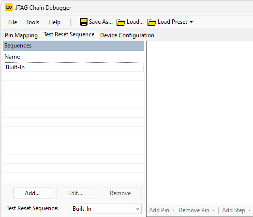
Figure 12: Adding a Test Reset sequence
Once the signals are in place, a waveform is created by adding a number of steps and then entering the signal transitions by using the mouse in the cell in which they are to occur, and moving the waveform to the required position. Transitions can also be edited by pressing the space bar, which toggles the state between driving high, driving low, and not driving (high-impedance). Other types of step in the waveform such as a TMS Reset can also be dragged into the desired position.
- The high impedance (tri-state) condition is represented by a mid-height line.
There are several good practices that should be followed when creating a reset sequence:
- nTRST: Although JTAG defines nTRST as an asynchronous signal, XJTAG has found that some devices do not behave correctly if nTRST's low-to-high transition occurs too soon after power-up. Furthermore, some manufacturers have implemented nTRST as a synchronous signal. For both reasons, it is recommended to include a Pulse nTRST step in the reset sequence which holds nTRST low for one TCK pulse before taking it high and then applying a second clock pulse as shown in Figure 13.
- TMS: It is good practice to include TMS in the reset sequence to ensure it is held high. This ensures that if the state machine of a device without a nTRST pin powers-up in an unusual state, clock edges will shift it towards its reset state rather than potentially executing an instruction.
TMS Reset
Test Reset sequences should end with a TMS reset step in order to put the JTAG controller into a known state before the next operation. The Built-In or Built-In (nTRST) sequence does this already, but you should make sure that any user-defined sequence you create includes a TMS reset step to ensure correct initialisation. This is normally placed at the end of the sequence. If you try to save a reset sequence without one in place, a warning message is displayed.
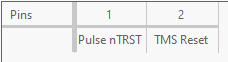
Figure 13a: Built-in (nTRST) sequence
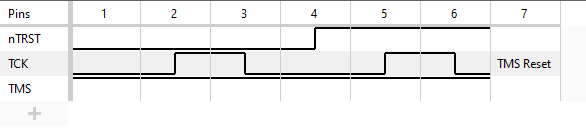
Figure 13b: Equivalent sequence waveform
- Not including a TMS reset can cause random failures due to bad initialisation; it is extremely rare not to need one, and it should only be omitted after detailed discussions with XJTAG Support.
- Provided Dynamic Chains are not being used, the test software expects the JTAG device to have placed the ID register (or bypass register if IDCODEs are not supported) between TDI and TDO after a reset. Devices do this automatically when they receive a TMS reset, and the sequence should therefore normally end with a TMS Reset to ensure the device is in the expected state.
- If Dynamic Chains are being used, the TMS reset may be required at a different point in the sequence.
- A few devices require extra steps to prepare them to have their ID register read, but this is very rare. If needed, this is done by using a Function Call step in the sequence to execute XJEase code.
Timing Considerations
Delays
Some devices require an input state to be held for a certain period of time. If required, a delay can therefore be inserted into the sequence by highlighting the relevant cell and adding or inserting a Sleep step, which allows you to set a sleep period in units of milliseconds.
- You cannot edit built-in sequences - if you are using a built-in sequence you will need to first create your own test reset sequence in order to add a delay.
Timing of signals
When driving signals in a Test Reset Sequence it is sometimes necessary to consider the effect of the output characteristics of the XJTAG controller together with the resistive and capacitive loading of the signal it is driving.
Consider the case shown in Figure 14, of a device with an nRST pin that is required to be held low before boundary scan tests can begin. For normal operation this pin has a pull-up to VDD and a capacitor to GND, in order to generate a power-up reset to the device.
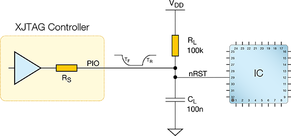
Figure 14: Example of driving an nRST pin
The output impedance of the XJTAG controller will influence the time taken to reach either a High or Low state according to the R-C time-constant of the controller source impedance (RS) and the load capacitance (CL).
In the case when the test reset sequence drives the nRST signal low the time taken to reach the low state will be approximately:
TF = RS × CL
TF = 50 × 100 × 10-9 = 5 μs
When the controller drives the signal high the time will be approximately the same, as long as its output impedance is the same for both a high and low output.
However, if the test reset sequence is using the pin as open-drain ie. driving low and going Hi-Z to achieve the High state via the pullup resistor RL, then the time taken for the nRST pin to reach a logic High and hence bring the IC out of reset is determined by RL and CL and will be approximately:
TR = RL × CL
TR = 100 × 103 × 100 × 10-9 = 10 ms
In cases such as these where timing is important to the success of the test reset sequence operation, it is necessary to add sufficient time delays in the sequence to allow valid logic levels to be reached.
- The reset waveform does not include timing information: each step is simply a transition, not a block of time. Adding an empty step will not add a delay because it will be ignored at run time - use a Sleep step instead.
For detailed information on the output impedance of XJTAG controllers please consult the datasheet for the XJTAG product you are using.
XJTAG v4.3.0