Using Explorer to Increase Test Coverage
If you're trying to maximise test coverage and find that a particular pin or net is not being tested, you can use Explorer to find the cause. It allows you to follow a path through the circuit, showing disable values and the levels of boundary scan access at each point. This will help identify reasons for particular pins or nets not being tested.
As an example, consider the circuit of Figure 9, where U1 and U2 are JTAG devices.
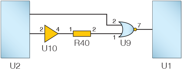
Figure 9: Example Circuit
For this circuit block, you would expect to have write and read access to every pin, and Connection Test should therefore perform full open- and short-circuit checks for every pin. However, if you found, for example, that there was no opens or shorts coverage for U9.7, you could use Explorer to trace the signal path back from that point until you found the cause, using the method described above in Following a Signal Path Using Explorer.
There are several possible reasons why a pin might not have the expected test coverage, and this section describes each of them:
- The impact of uncategorised devices on Connection Test
- The impact of incorrectly categorised devices on Connection Test
- How to check for disable values on a net
- Confirming the JTAG pin driving the net has the assumed capabilities
The Impact of Uncategorised Devices on Connection Test
The example of Figure 9 above will be used to demonstrate the impact of an uncategorised device on JTAG access.
If the Test Coverage screen shows that U9.7 is missing opens and shorts coverage, you would use Explorer to check the level of JTAG access to its two input pins, pins 1 and 2. In this example, pin 1 is found only to have read access, caused by being connected to a net that is currently identified as Excluded (see Figure 10 below). This suggests the lack of write access is because a device that JTAG wants to use to drive the pin is either uncategorised or is categorised as Excluded.
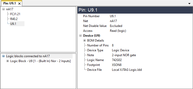
Figure 10: Pin That Will Not be Written in Connection Test Because the Net is Excluded
- When categorising devices, it is normal to start with passives and then work upwards through the list of uncategorised devices towards the ICs. Depending on the circuit, the situation can occur when categorising one device provides access to others, which then also need to be categorised. If you do not perform these additional categorisations as you go along, it can appear that JTAG access to a particular device is not possible and could lead to the incorrect decision to leave it untested. It is therefore best practice to check if new devices appear in already-cleared categories as you work through XJTAG's proposals.
To find which device is causing the lack of access, navigate backwards through the circuit as described above in Following a Signal Path Using Explorer until the cause of the problem is found. In this example, when the series resistor, R40, is reached, Explorer reports it as an uncategorised device:
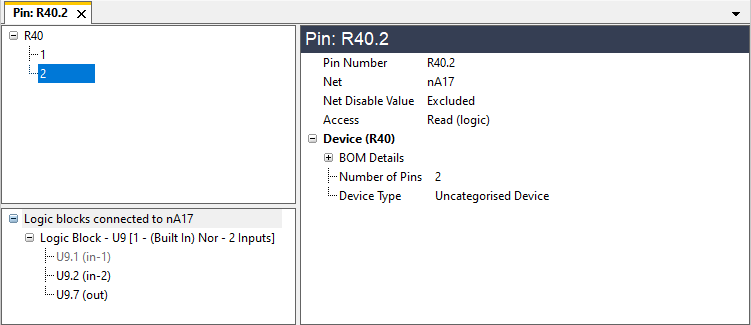
Figure 11: Explorer Identifying an Uncategorised Device
Once R40 has been correctly categorised, there will be read and write access via logic to pin U9.1, and a test coverage report will show Connection Test will perform full open- and short-circuit testing through that circuit block.
Checking Bus Disable Values & Constant Pins
Another possible cause for a pin not being tested during the connection test is if it's on a net that another device requires to be kept in a fixed state during the test (i.e., another device has imposed a disable value on the net). That can occur when, for example, the net is connected to another device's Output Enable pin and it is necessary to fix the state of that pin to prevent the device outputting during the connection test.
- Disable values (set in test device files) and constant pins (set in XJDeveloper's Constant Pins screen) both cause pins to be held in a fixed state. When a device is being explored, any disable values set by its own test device file are shown in the Disable Value column (see Figure 12 below). If a pin is connected to a net that is affected by a disable value set in another device's test device file or by a constant pin, the value will be shown in the Net Disable Value column.
- When exploring a net, Explorer will list all the pins on that net (see Figure 13 below). Beside each pin, any disable values or constant pins set for it will be shown in a column entitled Disable Value.
These disable values can reduce Connection Test's ability to control nets. They are displayed when a device is selected in Explorer as depicted in Figure 12:
Figure 12: Disable Values Displayed in Explorer
The upper right details pane has two columns for the different sources of disable values:
- The test file for the device itself may be imposing a disable value on the net (e.g. if the net is on the device's Output Enable pin, it may need to be held during the connection test to prevent the device driving nets). These are shown in the Disable Value column.
- The test file for another device may be imposing a disable value on the net (e.g. another device might need that net to be kept in a fixed state during the connection test to prevent it driving nets during the test). Constant pins (defined on XJDeveloper's Constant Pins screen) can also impact the ability to control a net, and any enabled constant pins will also show up as a net disable value. If another device or a constant pin imposes a disable value, it will be shown in the Net Disable Value column. If pins on that net can't be tested because of an uncategorised or excluded device in the access path, the net will be reported as Excluded.
- When a pin is a compliance pin (a pin on some JTAG devices that controls if it is in IEEE 1149.1 compatible mode), it will be shown as having a disable value because it cannot be used during boundary scan testing.
When exploring a net, every pin on that net is listed. If any of those pins are held in fixed states by disable values or constant pins, the Disable Value column will list their values:
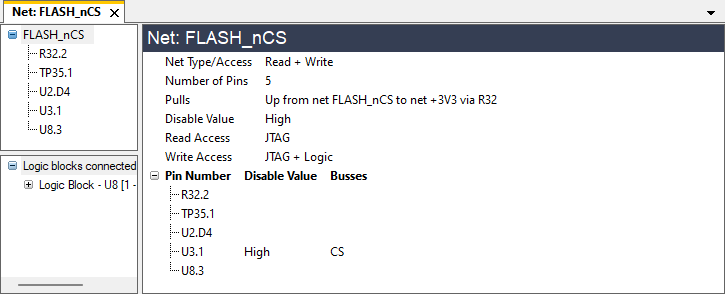
Figure 13: Exploring a Net Shows Disable Values & Constant Pins
Checking a JTAG Pin's Boundary Scan Capabilities
Another reason why XJTAG may be unable to test part of the circuit is if a JTAG pin used to access it does not have the necessary boundary scan capabilities. This could be because it is a Linkage pin (i.e. does not have any boundary scan cells) or because its boundary scan cells are not the type required for the test. For example, a test that requires a pin to have read access will obviously not work if the pin can only function as an output. Checking boundary scan cell types can therefore be important.
- Some JTAG ICs have compliance pins that must be held in a particular state for the device to be used in IEEE 1149.1 compliant mode; those pins cannot be controlled during a test.
If you have worked through the circuit and have reached a JTAG pin without finding the cause of the problem, you should check the pin's boundary scan functionality in Explorer's upper-right details pane. Figure 14 shows an example of a JTAG device's pin details. The pins that are shown as linkage cannot be used in the boundary scan test.
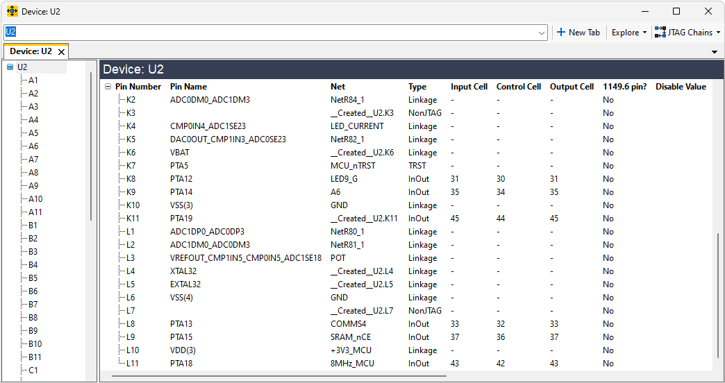
Figure 14: Checking a JTAG Device's Pin Capabilities
The Impact of Incorrectly Categorised Devices
Consider the circuit in Figure 15 below, in which there is a pull-up resistor on the output of the tri-stateable buffer.
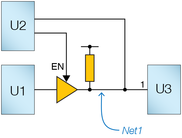
Figure 15: Circuit Using a Pull Resistor
If U1 and U2 are both JTAG devices, boundary scan can be expected to have both read and write access to pin 1 of U3 (U1 should give write access, and U2 should give both read and write). However, if the pull-up resistor is incorrectly categorised as a series resistor, XJDeveloper will believe that Net1 is shorted to the supply rail. The system will therefore only allow read access to U3.1 because it will never attempt to drive a net connected to power or ground.
To investigate the lack of test access on U3.1, Explorer can be opened to display details for the pin:
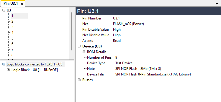
Figure 16 An Incorrectly Categorised Pull Resistor Causing a Net to be Considered Power
It can be seen that the net connected to pin 1 is being considered as a power rail, which is why the system will not allow the pin to be driven. To find the cause, use Explorer to work back through the circuit towards the JTAG device as described above in Following a Signal Path Using Explorer until the problem is identified.
- When a pin is connected to power or ground and can be read using boundary scan, it will be shown as having Read access, even though it will be identified as a power net. Its value will be checked during the connection test.
In this example, it will be found that the resistor connected to NET1 is providing a direct connection through itself to its other pin, which is connected to power (Figure 17). This shows the cause is that the resistor has been incorrectly categorised as a series resistor instead of a pull resistor.
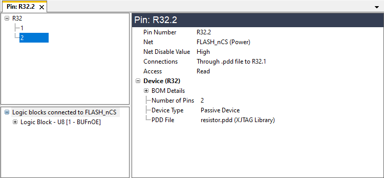
Figure 17: This Resistor Is a Direct Connection to Power, Not a Pull Resistor
Re-categorising the resistor as a pull device will correct the problem, and there will then be read/write access to pin U3.1.
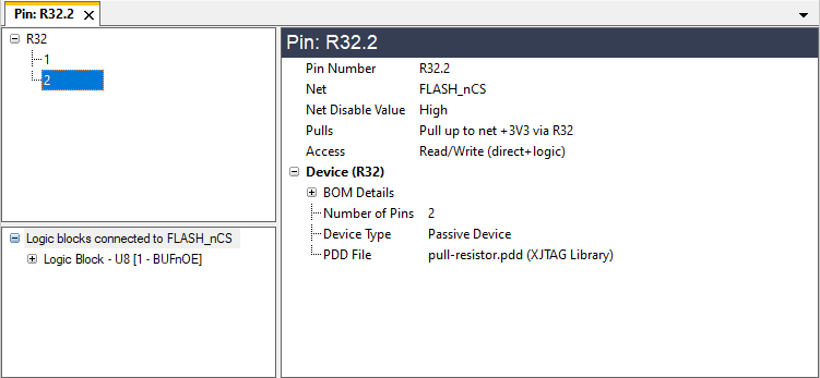
Figure 18: A Correctly Categorised Pull Resistor in Explorer
- When categorising a device with a test device file, if the access required by the test device file isn't available, XJDeveloper will flag the problem in the Warnings tab.
- Common categorisation mistakes include categorising a pull resistor as a series device, and selecting a model file for a logic device or resistor pack that has the wrong pin-out.
XJTAG v4.3.0