Configuration - Step 2
The second setup page allows you to select information about how the FPGA is connected to the flash and where it receives its clock.
For a typical FPGA the page looks something like this:
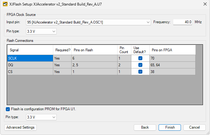
- FPGA Clock Source - XJFlash uses an external clock to allow it to run as fast as possible.
- Input pin - from the dropdown list, select the pin on your FPGA which is connected to the clock. For LVDS pins, the positive pin should be selected.
- Frequency - enter the frequency for the pin.
- Pin type - select the voltage level for the clock pin.
-
Flash Connections - XJFlash will attempt to automatically find the pins on the FPGA which are connected to the flash, and will show them in the table. In the example screenshot for SPI NOR flash, the necessary pins are SCLK, DQ and CS.
If XJFlash was unable to find the correct pins, they can be entered manually - untick the Use Default box and type in the correct pin in the column Pins on FPGA. For busses containing multiple pins, use a comma separated list from MSB to LSB.
All signals or busses which are required must be specified before continuing. Those marked as not required will be used if they are specified, otherwise they will be ignored.
- Configuration PROM tickbox - If the flash is a configuration PROM, tick the box.
- Pin type - select the voltage level for the flash connection pins.
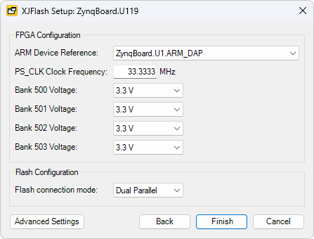
For a System on Chip (SoC) device, the pins on the device are unlikely to be configurable but there may be other settings for bank voltages and flash configuration. A typical example is shown here:
Advanced Settings
More settings are available in Advanced Settings, including constant pins and block RAM size.
Next Step
XJTAG v4.3.0