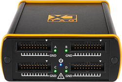
XJLink-PF40
XJLink-PF40 is a USB-connected JTAG controller used to link your PC to the Unit Under Test (UUT). XJLink-PF40 can connect to up to eight TAPs on the UUT.
Quick links:
Converting projects to use XJLink-PF40
If you have a project which was set up using an original XJLink or an XJLink2-based controller, it will probably need conversion in order to use an XJLink-PF40, because each connector on the XJLink-PF40 has 10 ground pins (all even-numbered pins), whereas the XJLink2 connector only has 2 ground pins (pins 10 and 20).
Connecting XJLink-PF40 to the UUT
The connection to the UUT is made using standard 20-way 0.1" (2.54 mm) connectors. The XJLink-PF40 has 4 of these connectors. On each connector, the odd numbered pins (1, 3, 5.. 19) are multipurpose and can be configured for a variety of functions. The even numbered pins (2, 4, 6.. 20) on the connector are ground pins, and at least one should be connected to the appropriate GND net on the UUT.
Pin mappings
The XJLink-PF40 has a configurable pin-out, using the odd-numbered pins of its connectors. The even-numbered pins are connected to GND.
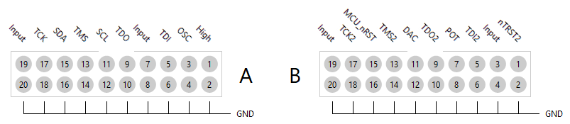
There is a pre-defined pin mapping for XJTAG's XJDemo v4 board available for the XJLink-PF40, which is loaded by selecting Load Preset on the Pin Mapping screen in XJDeveloper or in the JTAG Chain Debugger application. This pin mapping can be used as an example but the intention is that you can create your own pin mapping that suits your project.
The pre-set pin mapping for the XJDemo v4 board (which uses an adaptor board supplied by XJTAG to distribute the signals for its 2 TAPs across connectors A and B of the XJLink-PF40) is shown below:
Pin functions
All odd-numbered pins on each 20-way connector are multipurpose pins which means they can be configured to allow the use of a cable assembly between XJLink-PF40 and the UUT.
The even-numbered pins are Ground pins and are not configurable. At least one Ground pin from each connector must be connected to the UUT, preferably near to or on the same connector as where the TAP pins are connected.
All odd-numbered pins have a switching rate up to 166 MHz.
Pin types
There are many different ways that the multipurpose pins can be configured on an XJLink-PF40. The table below describes all of these pin types:
| Pin Type | Description |
|---|---|
| TDI (+ TDI2 ... TDI8) | This signal is the data input to a JTAG chain(s) on the UUT. There must be one TDI pin defined for each JTAG chain that the XJLink-PF40 is connected to. |
| TDO (+ TDO2 ... TDO8) | This signal is the data output from a JTAG chain. There must be one TDO signal defined for each JTAG chain that the XJLink-PF40 is connected to. |
| TCK (+ TCK2 ... TCK8) | This signal synchronises the other signals that make up the TAP. There must be a TCK connection to each JTAG chain the XJLink-PF40 is connected to; however these do not necessarily need to be separate connections. See Multiple TAP configuration below. |
| TMS (+ TMS2 ... TMS8) | This signal controls the operation of the TAP. There must be a TMS connection to each JTAG chain XJLink-PF40 is connected to; however these do not necessarily need to be separate connections. See Multiple TAP configuration below. |
| nTRST (+ nTRST2 ... nTRST8) | These are optional JTAG pins which are used by Test Reset Sequences to reset JTAG devices. Assigning a pin to one of these will ensure it is incorporated into the built-in sequence for the associated TAP. They may also be used as PIO pins in XJEase code and in the Test Reset Sequence. |
| PIO | This pin type allows direct control of pin(s) on the XJLink-PF40 either during a Test Reset Sequence or during XJEase testing. Pins of this type can also be used to measure frequency or voltage. |
| Low | This is a low signal driven by the XJLink-PF40; normally used for configuration of the UUT. |
| High | This is a high signal driven by the XJLink-PF40; normally used for configuration of the UUT. |
| Input | This signal type simply indicates that the XJLink-PF40 will not drive this pin during testing. It is the default setting for pins that have not been configured. |
| Oscillator Output | Pins assigned as Oscillator Output will output a square wave at the frequency defined in the Initial Frequency box. This frequency can then be modified any time using the SET_OSC_OUTPUT_FREQ XJEase statement. If the frequency is set to 0 Hz (either initially or by later use of XJEase) the output will be put in a high impedance state. |
| VREF | This input signal provides a voltage for the XJLink-PF40 to use as the output voltage level for the connector that the VREF pin is located on. A VREF pin can therefore be defined for each connector on the XJLink-PF40. |
| Tests Passed repeat signal | This signal indicates that the last set of tests that were run passed. It can be used to signal this to an LED or other test equipment. |
| Tests Running repeat signal | This signal indicates that tests are currently running. |
| Tests Failed repeat signal | This signal indicates that the last set of tests to run failed. |
| Run Button | This input signal allows the operator to start tests without needing to touch the PC, for example by placing a pushbutton on a test fixture. In XJDeveloper this functionality can be disabled using the Release XJLink if tests are not running option under Tools->Options->Hardware, in order to open other XJTAG applications without leaving the Run Tests screen in XJDeveloper. |
GND
The other, non-configurable, pin type is GND. Even numbered pins on each connector are connected to ground within the XJLink-PF40.
Every effort should be made to connect GND to the ground net on the UUT.
Bank and pin configuration
Output bank configuration
Each 20-way connector forms a voltage bank. The output voltage on each bank (odd-numbered pins) can be set between 1.2 V and 3.3 V in 0.1 V steps.
The output level of each voltage bank can also be set to mirror a value read from the UUT by setting a pin within the connector to be of type VREF. A VREF pin only sets the output level for the connector on which it is located, and each connector has its own output settings.
The voltage on a VREF pin will be sampled and applied to the XJLink bank at the start of testing, or just before performing any I/O operations.
Input pin configuration
By default, input pins use one of the LVCMOS switching levels (3.3 V, 2.5 V, 1.8 V, 1.5 V, 1.2 V), or can be set to a user defined level on a per bank basis. All input pins are 5 V tolerant.
Multiple TAP configuration
The XJLink-PF40 supports up to 8 TAP connections. Each connection has a TDI signal and a TDO signal, which are called TDI and then TDI2 up to TDI8, and similarly TDO, TDO2, and up to TDO8. The pin mapping can contain only one of each of these pins, and they must be paired, so TDO3 is always the pair of TDI3.
TAPs may be referred to by number - e.g. TAP 2 refers to the TAP connection based on TDI2 and TDO2, etc.
Each TAP connection must have a TMS pin and a TCK pin. The XJLink-PF40 supports 8 different TMS and 8 different TCK signals (named similarly to TDI/TDO pins). However multiple pins can be configured as a TMS or TCK signal and each pin with the same name will emit the same signal.
It is also possible for TMS and TCK pins to be associated with more than one TAP. When this is the case the TAPs sharing TMS and TCK signal (referred to as a TAP Group) are operated in sync with each other.
In XJTAG testing it is possible to run a test using only a subset of the chains that have been defined.
Multiple-TAP Limitations
Multiple-TAP configurations on the XJLink-PF40 are subject to some limitations:
- All pins of a TAP must be on the same connector on the front of the XJLink-PF40.
- Any single connector on the front of the XJLink-PF40 can contain pins from a maximum of 2 TAPs, although they do not have to be sequential - you could have TAP2 and TAP 6 on connector A.
- If TMS and TCK signals are shared between two TAPs, both TCK and TMS must be shared between the TAPs.
- TAPs which share signals must be sequentially numbered (e.g TAP 2 and TAP 3 but not TAP 2 and TAP 4)
Powering the Unit Under Test
Unlike an XJLink2 or derived JTAG controller, the XJLink-PF40 is not capable of supplying power to the UUT. Ensure that the UUT's power supply is enabled and that sufficient rise time is allowed for voltage rails before starting tests.
Measuring UUT frequencies and voltages using XJLink-PF40
The frequency or voltage can be read on any multipurpose pin, irrespective of its type. This measurement can be done using the JTAG Chain Debugger or through XJEase (using the PIN_FREQUENCY or PIN_VOLTAGE built-in functions, assuming you have an appropriate licence).
Status LEDs
Power
The XJLink-PF40 has a blue LED near the centre of the front panel which indicates that the unit is powered.
Status / Activity
Next to each port is an LED which indicates status:
- Green: Last test run passed
- Red: Last test run failed
- Flashing amber: Testing in progress
Design considerations for UUT connection
- At least one Ground pin (even-numbered pins) should be connected to Ground on the UUT from each connector in use on the XJLink-PF40.
- TCK ideally should be routed close to a ground signal in the cable to the UUT.
- The voltage output levels of the XJLink-PF40 should be set to match the connectors being used.
- The input level of the TDO pin of each TAP should be checked to match the final JTAG device in each chain.
- On the UUT, JTAG signals should be correctly terminated, to reduce the potential for reflected signals to cause glitches in JTAG operation. XJTAG produces DFT guidelines documents in several languages which give details of how best to terminate signals - please download them from the XJTAG website or contact XJTAG support to obtain a copy.
- Understand the limitations of multiple-TAP configuration of the XJLink-PF40.
- If you need your UUT to work with both XJLink2-series devices and XJLink-PF40, consider the differences in connector pin-out of both devices to make sure there are no problems.
Self-test functionality
If you wish to verify that your XJLink-PF40 is functioning correctly, you can run tests on the unit via the XJLink Manager utility.
Technical specifications
The technical specifications for the XJLink-PF40 can be downloaded from the XJTAG website.
XJTAG v4.3.0