Following Signal Paths using Explorer
Explorer allows you to trace the signal path through a circuit. This is useful when trying to discover why a pin does not have the JTAG access you expected because you can use it to work backwards through the circuit towards the JTAG pin that should be driving it. As you go, you can check details of each net and pin.
If you click on a pin in the navigation panel, the upper right section in the Explorer window will display the pin's details, including the net to which it's connected; double-clicking a pin will jump Explorer to that net and show everything connected to it. The example of Figure 3 demonstrates this progression and how to use it to navigate through the circuit.
The example starts at (A) after searching for U1. All of U1's pins are listed in the upper left navigation panel, and details about U1 are shown in the upper right details section. To trace how a signal gets to pin U1.24, for instance, click on that pin in the navigation panel. Details of pin 24 are now displayed, and it can be seen in (B) that it is connected to a net named DECODE.
Double-clicking on pin 24 will now jump to a display of information for the DECODE net (C). As shown in the example below, the navigation panel now shows all the pins connected to DECODE.
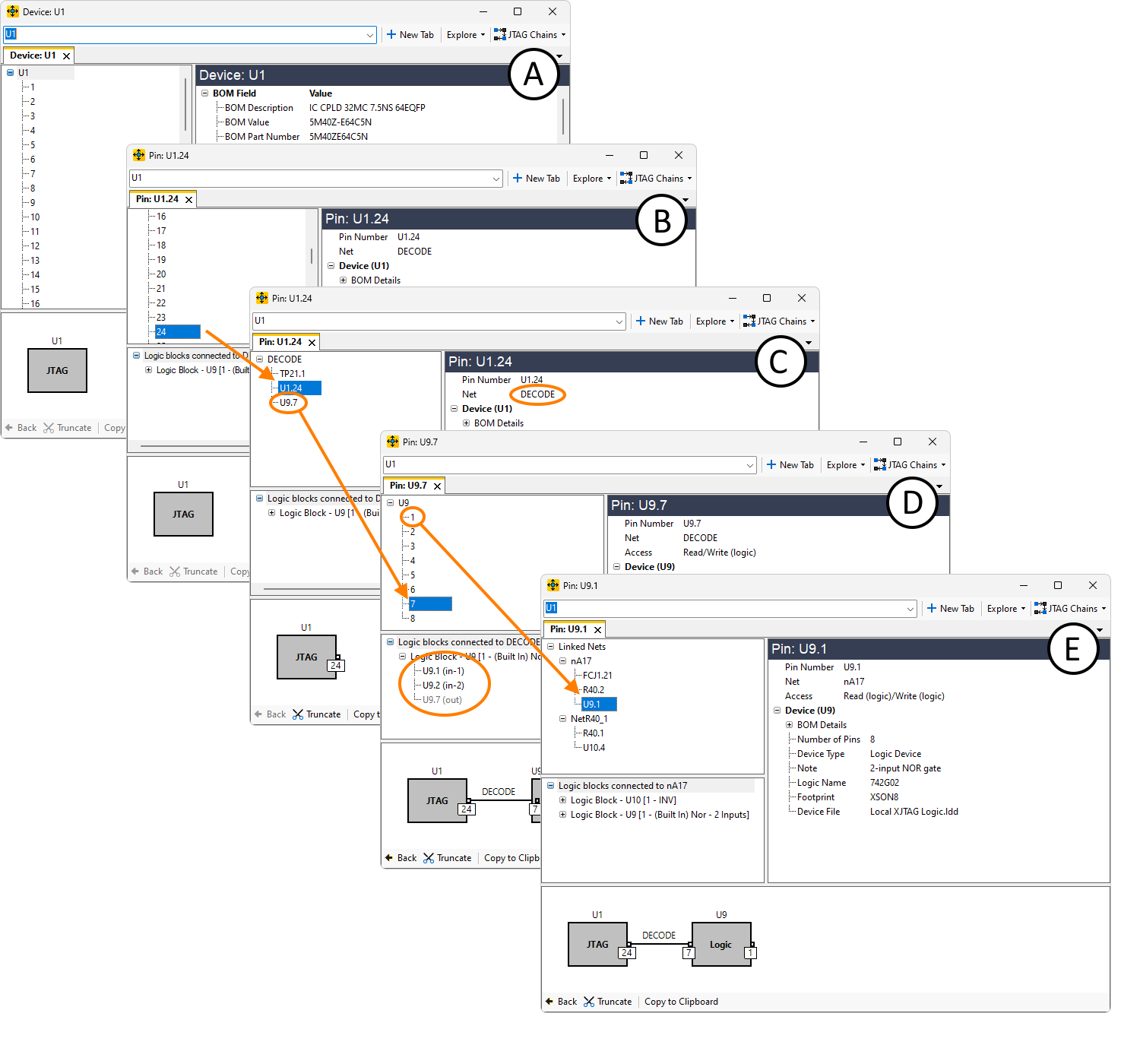
Figure 3: Tracing a Signal Through the Circuit
It is clear from (C) that the signal for pin U1.24 comes from pin U9.7. Therefore, to continue tracing the signal, double-click U9.7, and Explorer will jump to a display of information about that pin (D). Because U9 is a logic device, XJDeveloper knows that the relevant inputs are pins 1 and 2, and it displays that information below the navigation panel. To continue, decide which input to follow first and double-click on that pin.
If the device is not logic, the possible input pins will not be shown in the same way but, instead, you can look at the list of the device's pins in the details section to decide which input to follow.
- To view any of these points on the schematic, right click a reference to a pin, device, or net and select Show in Schematic Viewer from the context menu.
In this example, the signal path to pin U9.1 is being explored first: double-clicking on that pin jumps Explorer to a display of all the nets connected to it (E), from which the next step can be chosen.
You can continue following the signal back through the circuit in this way. Each time the signal passes through a pin, the graphical representation of the signal path at the bottom of the window is extended to show the route that has been taken. At any point, you can retrace your steps by clicking the Back button at the bottom of the window.
Examples of using Explorer in this way to find why Connection Test is not getting the expected test coverage are provided in subsequent sections.
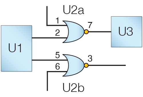
- Explorer does not stop you deviating off the true signal path. For example, in this circuit, when exploring U2 from pin 1, it would be possible to jump next to U2b's output by mistake. Explorer will not stop you making this mistake. It is therefore always important to check you are moving to an appropriate pin on the device being explored.
Quick Navigation Using the Graphical Navigation Panel
The graphical navigation panel gives a diagrammatic representation of the signal path that has been followed. As well as providing a useful reminder of the route that has been taken to the current net or pin, it can be used as a means of quick navigation.
Consider the example described above in Figure 3. After the output of the logic gate was reached (4), a decision had to be taken on whether to continue by working back from the input on pin 1 or the input on pin 2. Tracing the signal back through the circuit from pin 1 would end up with a diagram similar to that shown in Figure 4:
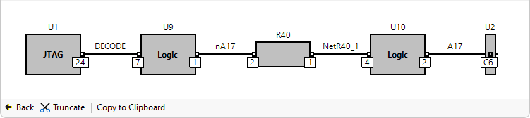
Figure 4: Explorer's Graphical Navigator
To display information about any of the devices, pins, or nets, click the item in the diagram, and the details will be displayed in Explorer's upper right section. This provides an easy way to check JTAG access, disable values, etc. at points along the signal path.
Once a particular path has been investigated, it may be necessary to return to the logic gate and explore the other input. The graphical navigator provides a quick way to jump back to that place in the path: select the device you want to return to (in this case U9). All the pins of the device will then be shown in the navigation panel, and you can double-click on the other input (which, in this example, is pin U9.2). This progression is illustrated in Figure 5 below. You can then continue to trace back the signal from this other input.
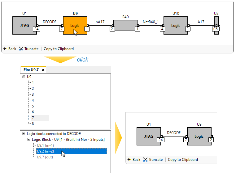
Figure 5: Retracing your Steps Through the Signal Path
While tracing a signal, if you jump between two nets that aren't directly connected, the jump will be indicated by a dotted line as shown in the example of Figure 6 below. This can happen, for example, when two nets are linked by a low value series resistor, and you jump directly to a pin on the other net rather than going through the linking device.
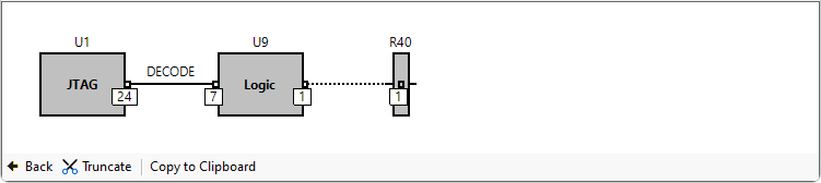
Figure 6: How the Graphical Navigator Indicates a Jump in the Signal Path
XJTAG v4.3.0