XJLink2
XJLink2 is a USB-connected JTAG controller used to link your PC to the Unit Under Test (UUT). XJLink2 can connect to up to four TAPs on the UUT.
Quick links:

Converting Original XJLink projects to use XJLink2
Nearly all projects should work when switching from using an original XJLink to an XJLink2. A project will however produce a runtime error if pin 10 on the pin mapping is used as anything other than a low or input. This is because pin 10 is a Hard Ground pin on the XJLink2.
Connecting XJLink2 to the UUT
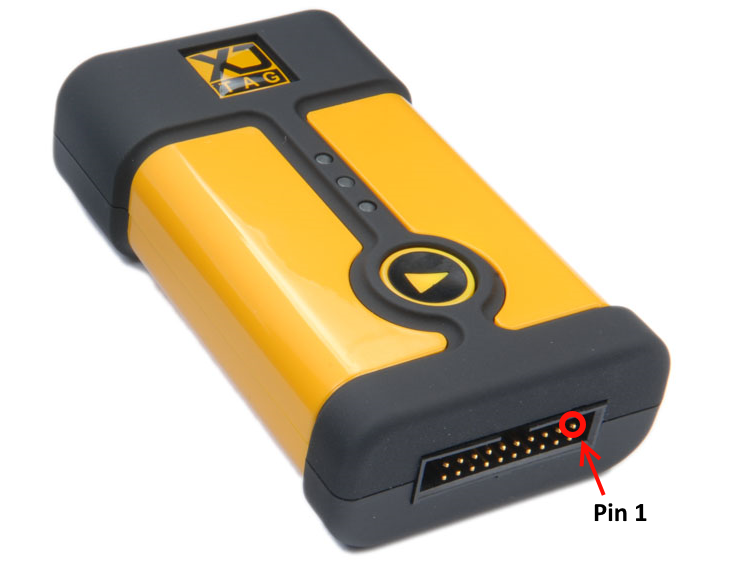
The connection to the UUT is made from a standard 20-way 0.1" (2.54 mm) connector. Most of the pins on the connector are multipurpose and can be configured for a variety of functions.
Pre-defined Pin Mappings
The XJLink2 has a configurable pin-out on the JTAG connector.
There are a number of common pin mapping configurations pre-defined in XJTAG:
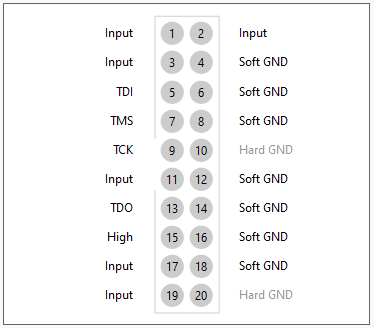
The default XJTAG pin mapping for a single TAP on XJLink2 is shown below:
|
|
Custom pin mappings
Where the pins on the UUT do not match one of the pre-defined configurations, a custom layout of TAP pins can be configured on the XJLink2. This pin mapping description can then be stored in a pinmap configuration file, which then can be used in any of the XJTAG tools.
XJLink2 pin functions
The function of most of the pins on the 20-way connector can be configured to allow the use of a simple cable assembly between XJLink2 and the UUT.
The only non-configurable pins are pins 10 and 20 which are Hard Ground pins. All other pins are multipurpose pins.
All pins have a switching rate up to 166 MHz.
Pins 1 and 11 can alternatively be used to supply power to the UUT from the XJLink2. Up to 100 mA can be supplied in total, split between these two pins.
Pin types
There are many different ways that the multipurpose pins can be configured on XJLink2. The table below describes all of these pin types:
| Pin Type | Description |
|---|---|
| TDI (and TDI2, TDI3, TDI4) | This signal is the data input to the JTAG chain(s) on the UUT. There must be one TDI pin defined for each JTAG chain that the XJLink2 is connected to. |
| TDO (and TDO2, TDO3, TDO4) | This signal is the data output from a JTAG chain. There must be one TDO signal defined for each JTAG chain that the XJLink2 is connected to. |
| TCK (and TCK2, TCK3, TCK4) | This signal synchronises the other signals that make up the TAP. There must be a TCK connection to each JTAG chain the XJLink2 is connected to; however these do not necessarily need to be separate connections. See Multiple TAP configuration below. |
| TMS (and TMS2, TMS3, TMS4) | This signal controls the operation of the TAP. There must be a TMS connection to each JTAG chain XJLink2 is connected to; however these do not necessarily need to be separate connections. See Multiple TAP configuration below. |
| nTRST (and nTRST2, nTRST3, nTRST4) | These are optional JTAG pins which are used by the Test Reset Sequence to reset JTAG devices. Assigning a pin to one of these will ensure it is incorporated into the built-in sequence. They may also be used as PIO pins in XJEase code and in the Test Reset Sequence. |
| PIO | This pin type allows direct control of pin(s) on the XJLink2 either during a Test Reset Sequence or during XJEase testing. Pins of this type can also be used to measure frequency or voltage. |
| Low | This is a low signal driven by the XJLink2; normally used for configuration of the UUT. |
| High | This is a high signal driven by the XJLink2; normally used for configuration of the UUT. |
| Input | This signal type simply indicates that the XJLink2 will not drive this pin during testing. It is the default setting for pins that have not been configured. |
| Power | Pins 1 and 11 can optionally supply power. |
| RTCK | Some devices require an RTCK pin to be defined to operate correctly. Multiple pins can be defined as RTCK to operate with multiple devices requiring RTCK. However, the RTCK implementation in the XJLink2 is not compatible with dynamic chains/multiple clock signals or optimised scans mode. |
| Oscillator Output | Pins assigned as Oscillator Output will output a square wave at the frequency defined in the Initial Frequency box. This frequency can then be modified any time using the SET_OSC_OUTPUT_FREQ XJEase statement. If the frequency is set to 0 Hz (either initially or by later use of XJEase) the output will be put in a high impedance state. |
| VREF | This input signal provides a voltage for the XJLink2 to use as the output voltage level for both output voltage banks. VREF cannot be selected if VREF1 or VREF2 are in use. |
| VREF1 | This input signal provides a voltage reference for the XJLink2 to use as the output voltage level for Bank 1. VREF1 cannot be selected if VREF is in use. |
| VREF2 | This input signal provides a voltage reference for the XJLink2 to use as the output voltage level for Bank 2. VREF2 cannot be selected if VREF is in use. |
| Soft Ground | Even numbered pins can be set as soft ground pins; these are programmatically connected to ground within the XJLink2 with a very low resistance (less than one ohm). To achieve the best signal integrity, as many soft ground connections as possible should be made between the UUT and XJLink2. |
| Tests Passed repeat signal | This signal has the same function as the Pass LED on XJLink2 and is set High when the LED is illuminated. It can be used if an XJLink2 is embedded in a piece of test equipment to make the LED output available elsewhere. |
| Tests Running repeat signal | As above but for the Running LED on XJLink2. |
| Tests Failed repeat signal | As above but for the Failed LED on XJLink2. |
| Run Button | This is used to extend the Run Button input on the XJLink2 to work with an external push-button or other trigger. In this case, the pin on the XJLink2 should normally be held low; testing will start when the pin voltage is set high. |
Hard Ground
The other, non-configurable, pin type is Hard Ground. Pins 10 and 20 are connected to ground within the XJLink2.
Every effort should be made to connect pins 10 and 20 to ground on the UUT.
Bank and pin configuration
Voltage Banks
The pins on the 20-way connector are divided into two banks of ten; pins 1 to 10 make up Bank 1 and pins 11 to 20 make up Bank 2. The output voltage on each bank can be set between 1.1 V and 3.5 V in 0.1 V steps; these voltage settings are accurate to within 3 %.
The output voltage levels can also be set to mirror a value read from the UUT; this is achieved by setting a pin within the bank to be of type VREF. The voltage driven onto that pin from the UUT is then used to derive the bank voltage.
N.B. The voltage on a VREF pin will be sampled and applied to the XJLink bank(s) at the start of testing, or just before performing any scans.
Output pin configuration
The drive strength and slew rate of the output pins can be configured to allow high speed, high quality JTAG signals.
Drive strength options
The drive strength determines how much current is driven out of the XJLink2 to achieve valid logic levels under different loads. A drive strength can be set for each output pin individually.
Drive strength is defined with respect to the termination of the signal to be driven. The termination options will vary depending on the bank voltage for the selected output pin. Select the most relevant match to the input termination of the net on the UUT.
Slew Rate
Each output pin can have one of three slew rates that sets the rise and fall times of the signals from the XJLink2.
- Slow - If a JTAG chain has a signal integrity issue then it is often beneficial to select Slow as the slew rate and reduce the TCK frequency. Slow should only be used with TCK frequencies of less than 33 MHz at 3.3 V or 10 MHz at 1.2 V.
- Medium - This slew rate works in most situations and is the default value.
- Fast - This slew rate can be useful on high speed TCK systems, generally above 50 MHz.
Input pin configuration
By default, input pins use one of the LVCMOS switching levels (3.3 V, 2.5 V, 1.8 V, 1.5 V, 1.2 V), but can optionally be set to a user defined level on a per bank basis. All input pins are 5 V tolerant.
Multiple TAP configuration
The XJLink2 supports 4 TAP connections. Each connection has a TDI signal and a TDO signal, which are called TDI, TDI2, TDI3, TDI4, and similarly TDO, TDO2, TDO3 and TDO4. The XJLink2 pin mapping can only contain one of each of these pins, and they are paired, so if there is a TDI3 there must be a TDO3.
Each TAP connection must also have a TMS and a TCK pin. The XJLink2 supports 4 different TMS and 4 different TCK signals and these are named TMS, TMS2, TMS3 and TMS4 (similarly for TCK pins). However, multiple pins can be configured as a TMS or TCK signal and each of these pins will emit the same signal. Also, TMS and TCK pins can be associated with more than one TAP group, meaning that the two TAP groups either share TMS/TCK signals or they should be operated in sync with each other.
This means, for example, that it is possible to have 4 sets of TDI/TDO signals operating from a single TMS and single TCK signal, or it is also possible to have a setup where TDI/TDO and TDI2/TDO2 will share the TMS and TCK signals, while TDI3/TDO3 uses TMS2 and TCK2.
In XJTAG testing it is possible to run a test using only a subset of the chains which have been defined.
Powering the Unit Under Test from an XJLink2
The bank voltage can be output via pin 1 for Bank 1 and pin 11 for Bank 2 to power the UUT. Up to 100 mA is available in total; this can be split between the two banks.
The XJLink2 uses a soft start on its power pins to reduce the potential for overloading the current that can be supplied through USB. This will not be a problem provided the UUT does not need any additional time for its power rails to rise to a valid level. If the UUT also has a soft start (such as the XJIO board) then a delay must be inserted before communication is initiated. To do this, the first step in the Test Reset Sequence should be a sleep of an appropriate length for the UUT. As an example, the XJIO board needs a sleep time of 200 ms in the Test Reset Sequence.
Measuring UUT frequencies using XJLink2
The Frequency on any multipurpose pin can be read irrespective of its type. This measurement can be done using the JTAG Chain Debugger or through XJEase (assuming you have an appropriate licence).
Measuring UUT voltages using XJLink2
The voltage on any multipurpose pin can be read irrespective of its type. This measurement can be done using the Chain debugger or through XJEase (assuming you have an appropriate licence).
Run button
The XJLink2 has a button, which allows the user to start tests without needing to touch the PC. This functionality can be disabled in XJDeveloper using the Release XJLink if tests are not running option under Tools->Options->Hardware, in order to open other applications without leaving the Run Tests screen in XJDeveloper.
Status LEDs
The three status LEDs on the XJLink2 show testing status. If the yellow LED is flashing, tests are currently running. If the last test run failed (or was stopped prematurely), the red LED will be active. If the last test run passed, the green LED will be active. In Group Test mode in XJRunner, the relevant LED on all included XJLinks continue to flash until all test runs have ended.
If running in XJDeveloper and the Release XJLink if tests are not running option under Tools->Options->Hardware is set, then the red or green status will only be briefly shown, and the LEDs will all turn off when the hardware is released, indicating that other programs can control it.
Design considerations/troubleshooting
- XJLink2 Hard Ground pins (10 and 20) should be connected to Ground on the UUT.
- TCK should be on a pin next to the Hard Ground pins on the XJLink2 (pins 9, 11 and 19). If this is not possible then both adjacent pins should be Soft Ground pins.
- The voltage level of the XJLink2 should be set to match the board.
- On the UUT, JTAG signals should be correctly terminated, to reduce the potential for reflected signals to cause glitches in JTAG operation. XJTAG produces DFT guidelines documents in several languages which give details of how best to terminate signals - please download them from the XJTAG website or contact XJTAG support to obtain a copy.
Self-test functionality
If you wish to verify that your XJLink2 is functioning correctly, you can run tests on the unit via the XJLink Manager utility.
Technical Specifications
The technical specifications for the XJLink2 can be downloaded from the XJTAG website.
XJTAG v4.3.0